Chips are everywhere: from our mobile phones and automobiles to cloud servers for artificial intelligence, all of which seem to get faster, smarter, and better with each generation. Creating more powerful chips typically involves shrinking transistors and other components and packing them more closely together. As chip features become smaller, however, the incumbent materials may no longer achieve the same performance at the desired thickness and new materials may be needed.
Lam has pioneered a new deposition technology called SPARC for a new class of silicon carbide films with improved electrical insulating properties. Importantly, they can be deposited in ultra-thin layers and still have the robustness needed to survive downstream processing, even through the demanding steps needed to create high aspect ratio structures. Combining Lam’s unrivaled plasma capability with chemistry and process engineering, SPARC has enabled performance and technology scaling of advanced logic and DRAM.
Improving logic device performance
A key logic application for SPARC is for FinFET spacers. As shown in the flow below, a spacer film is deposited on incoming gates and fins. The film must follow the exact contours of the existing structure (or be conformal), as well as uniform in thickness. It must additionally have excellent adhesion to the layer below and be without pinholes or other defects. And it must be easily removable from everywhere except its desired location at the gate sidewalls.
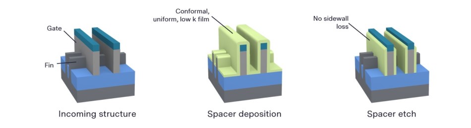
The film itself has requirements. As transistors scale down, there is increasing capacitive coupling in the gate module that degrades overall transistor performance. The SPARC carbide films are excellent examples of a novel class of better electrical insulating materials, so called “low-k films” that are needed to minimize such coupling. Existing low-k films are typically fragile, unable to withstand the harsh chemistries used in subsequent steps. Not surprisingly, they can lead to poor overall chip performance.
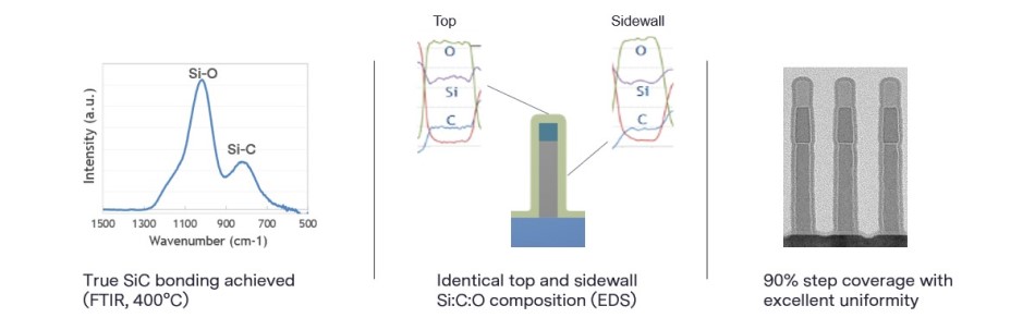
Lam’s SPARC technology delivers uniform, robust low-k films that are conformal not only in terms of thickness but also composition inside of features. The SPARC film is deposited gently, without direct plasma that damages the sensitive devices beneath. It does so by using radicals generated by a unique reactor with remote plasma and a novel precursor. Unlike direct plasma-enhanced atomic layer deposition (ALD) films, it lends itself to easy tuning of film composition to optimize for damage prevention and dry or wet etch selectivity. The resulting film is thin, pinhole-free, and can maintain correct silicon-carbon (Si-C) bonding structure – and hence, its dielectric properties and robustness – through the rest of the chipmaking process.
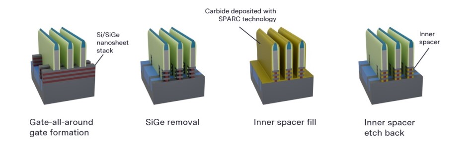
With the advent of gate-all-around (GAA) architecture, the value of Lam’s SPARC technology is even more evident. The new inner spacer application requires a material to reduce the parasitic capacitance of the device – that is, to reduce the interference between the devices. The film must also act as a protection layer for the epitaxially processed source/drain during SiGe channel release process. SPARC-deposited films bring key properties to this application, including low-k value, conformality, high pattern loading, uniform thickness, excellent etch selectivity to Si-based, oxide, carbon type of materials, and very low leakage in device.
It is good for DRAM, too
As devices scale, there is continuing effort to reduce the capacitance between the bit line and capacitor contact in order to maintain good signal/noise for bit sensing. Bit line aspect ratio increase is also making it challenging for conventional methods of deposition to succeed. A significant component of the bit line capacitance is coupling between the bit line and the storage node contact (SNC), which is increasing as these devices come closer to pack more bits per unit area to reduce DRAM cost and increase density. To reduce such a coupling, SPARC-deposited low-k spacer material has been critical since 1x nm technology node.

The ideal low-k thin film
The silicon-carbide-oxide (SiCO) films created with SPARC, or single precursor activated radical chamber, technology are dense, robust, with low dielectric constant ~ 3.5-4.9, low leakage and excellent thickness and compositional conformality. Across a wide range of temperatures, 250°C to 600°C, the carbon is fully cross-linked with very little to no terminal methyl groups, providing the film with both thermal and chemical stability compared to other films such as SiOC or SiOCN or SiCN.
Within the SPARC SiCO family, the remote plasma, unique precursor and process space enable a wide range of composition tuning. In addition, these SPARC SiCO films have zero WER (wet etch rate) in typical wet chemistries such as dilute hydrofluoric acid and hot phosphoric acid, thus also offering near-infinite wet etch selectivity. These films are also continuous and pinhole-free at less than half the thickness of typical alternatives.
Because of these features, the SPARC SiCO films are an attractive choice to minimize film thickness in certain spacer applications. Given its significant wet selectivity or plasma damage prevention of high aspect ratio stack materials, these films enable air-gap formation, capacitance coupling reduction, and protection of process elements in the high aspect ratio stack that are readily oxidized or damaged. SPARC technology has been adopted by all major logic/foundry and DRAM manufacturers at leading technology nodes. The next-node application space is expected to increase with increasing integration and performance scaling challenges and higher aspect ratios.