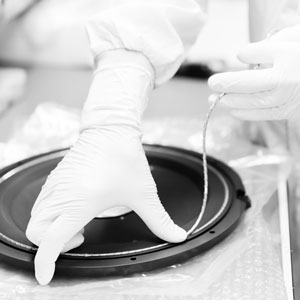
At Lam Research, our manufacturing employees play a vital role in building some of the most complicated products in the world – chipmaking equipment that is used to make the devices we enjoy every day. From production managers and pilot test engineers to assembly specialists and test technicians, these professionals truly enjoy the variety of activities and challenges they face each day at work.
Whatever ideas you may have about manufacturing, you might be surprised to learn what it’s like in a high-tech environment. At our production sites, collaboration is a big part of every position. For example, at our 24/7 facilities, detailed daily status passdowns from the previous shift ensure very aggressive schedules stay on track. Team members also work regularly with Lam’s network of global suppliers and alongside our Product Group engineers to identify and address a wide range of production challenges. In addition, our practices involve complex merge-in-transit processes: individual modules are manufactured at specialized facilities around the world, then later assembled at chipmakers’ fabs to significantly shorten the production timeline for our customers.
These complex activities must be expertly managed for our diverse product lines. To accomplish this, we operate four facilities around the globe, each focusing on manufacturing certain types of Lam equipment:
Livermore, California: Located near the heart of the Silicon Valley, about half an hour’s drive from our headquarters in Fremont, this state-of-the-art facility manufactures our etch products, offering advanced technologies for conductor, dielectric, and atomic-layer etching (ALE) applications.
Tualatin, Oregon: About 15 miles from Portland, this 58-acre campus produces Lam’s deposition systems – electrochemical deposition (ECD) and chemical vapor deposition (CVD) for metal films, plasma-enhanced CVD (PECVD) for dielectric films, and atomic layer deposition (ALD) – along with our photoresist strip products.
Villach, Austria: Surrounded by mountains, lakes, and natural mineral springs, Villach is home to development and manufacturing of our spin clean products, which are used to remove unwanted materials from the wafer throughout the chip-making process.
Osan, South Korea: This advanced manufacturing facility in Asia produces our plasma bevel clean systems along with platforms and process modules for some of our etch and deposition product lines.
Interested in joining us? Learn more at lamresearch.com/careers.