| Su | Mo | Tu | We | Th | Fr | Sa |
|---|---|---|---|---|---|---|
| Su | Mo | Tu | We | Th | Fr | Sa |
|---|---|---|---|---|---|---|


 |Apr 23, 2024|
Lam plays a significant role in plasma science by collaborating with researchers, supporting the Allis Prize, and employing physics, chemistry, and engineering students and experts.
-
 |Apr 22, 2024|
A key component of Lam’s strategy is improving the energy efficiency of our products

 |Apr 16, 2024|
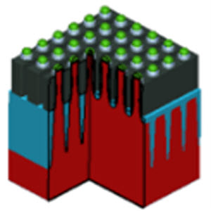
Abstract In this article, we demonstrate a pathfinding technique for a novel Vertical DRAM technology. First, we identify important process parameters (defined by current semiconductor production...

 |Apr 12, 2024|
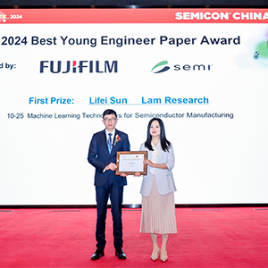
Li Fei Sun won for her paper on smart tools and ML solutions in semiconductor manufacturing In the past four years, Lam engineers have won the top award three times At Lam Research, we take pride...
-
 |Mar 26, 2024|
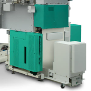
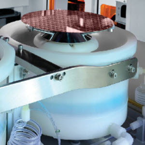
Introducing Pulsus, Lam's cutting-edge pulsed laser deposition tool. PLD enables specialty technologies like RF filters and MEMS microphones.
-
 |Mar 21, 2024|
There are still many challenges to be overcome before CFET designs become mainstream, but this new 3D architecture represents a promising new direction for the future of computing.
-
 |Mar 19, 2024|
Interest in artificial intelligence is driving data storage expansion for memory makers. Advancements in semiconductor manufacturing etch and deposition, and advanced packaging are playing a...
 |Mar 11, 2024|
One-of-a-kind contest supports semiconductor startups with investment and exposure
 |Mar 4, 2024|
Driving the news: Lam was named one of the World’s Most Ethical Companies® by Ethisphere–for the second year in a row. Lam is the only wafer fabrication equipment provider on this year’s...
-
 |Mar 1, 2024|
Dee’s career journey took on unexpected roles in engineering, quality, and operations She oversees the manufacturing operations across two facilities at Silfex I didn’t plan to work in...