Etch Essentials: The Building Blocks of AI Era Microchips (Semi 101)
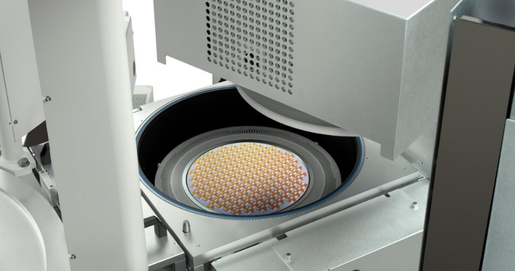
Lam Research’s Flex® tool uses dielectric etch; capable processes include ALE and RIE.

The Semi 101 series is a beginner’s guide to understanding microchips and the semiconductor industry – from components to processes and everything in between.
The artificial intelligence era depends on the storage infrastructure needed to run advanced technology, such as generative AI. The performance requirements for these AI innovations are pushing NAND devices to quickly scale to 400 vertically stacked layers and beyond.
Going vertical requires precise etching and novel chemistry. For decades Lam has been an industry leader in addressing key challenges in this process—etching deeper, faster, as well as enabling complicated lateral and vertical scaling. Our unique solutions allow customers to build next-generation chips that power AI and leading-edge technologies.
Modern silicon chips feature complex circuit patterns that conduct electricity through millions and even billions of transistors (a basic building block of electronics that switches electrical signals and power) and other types of devices. Some transistors are no wider than tens of silicon atoms.
To create these circuit patterns, a precise removal of silicon and other materials from the wafer surface forms a path. This process is repeated again and again, creating layers of circuit paths.
There are two main categories of etching in semiconductor manufacturing:
In wet etching, a wafer is etched by a liquid solution containing etching chemicals. Wet etching relies on chemical reactions to remove materials on the wafer and is typically isotropic, meaning the etch rate is the same between the vertical direction and the horizontal direction.
Advanced process technologies rely more on dry etching to form desirable patterns and shapes on wafers. Dry etching uses gases and is typically conducted under a vacuum, where the volatility of etch byproducts is higher and can be pumped out.
Cryogenic etching is a process, initially developed in the 1980s, that is re-emerging as a method of dry etching. The etch process is carried out at a low on-wafer temperature, typically below 0 degrees Celsius, with the temperature control unit operating at even lower temperatures. Cryogenic etching helps increase adsorption of reactive species while limiting the lateral etch rate.
Now that we’ve discussed the fundamentals of etching, let’s talk about the tools that perform these tasks. Etch tools are historically categorized into conductor etch tools and dielectric etch tools. With new technological inflections like FinFET and GAA, selective etch is emerging as a third etch tool segment.
Etching removes material through two basic mechanisms:
More advanced etching mechanisms:
As chipmakers continue scaling down their chips, the ability to etch precise channels is crucial for maintaining chip yield, effectiveness, and performance. Lam offers many product families for etch systems:
Kiyo® - Conductor Etch - Transformer coupled symmetric chamber design and advanced plasma pulsing capability for market leading results across the wafer.
Vantex™ - Dielectric Etch - Highest aspect ratio etching with tight CD (critical dimension) control and selectivity. Repeatable wafer-to-wafer performance enabled by advanced Equipment Intelligence®.
Flex® - Dielectric Etch - Small volume confined plasma with advanced RF pulsing for profile control and high mask selectivity.
Selis® - Selective Etch - High pressure ICP (inductively coupled plasma) source with high radical density; enabling isotropic selective etch with high throughput.
Syndion® - TSV Etch - Transformer coupled symmetric chamber design with fast gas switching for market leading results.
GAMMA® - Stand-Alone Strip - Large chamber volume with flexible high gas flow configurations, and multiple process stations for low defectivity and high productivity.
Versys® - Metal Etch - Metal L/M/N series provide critical CD, profile, and selectivity required for advanced BEOL (Back End of Line) patterning applications.
Glossary
Adsorption refers to the process by which molecules or atoms from a gas or liquid adhere to the surface of a solid material.
Aspect ratio refers to the ratio between the depth and the width of a structure. High aspect ratio structures are typically very tall with very small openings at the top.
Capacitively coupled plasma is a type of plasma generated between two parallel electrodes in a vacuum chamber.
Directionality refers to the property or characteristic of something that shows, has, or flows in a specific direction.
Dissociation is breaking the bond(s) of a molecule into smaller and more reactive components, also known as radical species.
Etch by-products are the secondary product formed during the etching process that can be pumped out when they are volatile.
Etch rate represents the speed at which material is removed during the etching process.
FinFET, Fin Field Effect Transistor, is a type of non-planar or "3D" transistor used in the design of modern processors.
Inductively coupled plasma is a type of plasma source in which the energy is supplied by electric currents that are produced by electromagnetic induction.
Pattern collapse refers to forces causing bending or mechanical instability of the photoresist layer, rendering the patterned features unusable for subsequent pattern transfer steps.
Radical species are highly reactive chemical entities that participate in chemical reactions during plasma etching, leading to material removal and surface modification.
RF pulsing refers to the technique of modulating radio frequency (RF) energy in a pulsed manner rather than continuously.
Selectivity refers to the difference in etch rate between two materials during an etching process.
Volatility is the tendency of a substance to evaporate at nominal temperatures.