-
about
-
products
-
customer support
-
careers
-
investors
-
newsroom
-
Languages
- MyLam

Blog
Driving the news: Lam Research earned the 2025 SEMI Award for North America for our pioneering cryogenic etch technology, Lam Cryo 3.0. SEMI recognized Lam at SEMICON West for driving the next generation of 3D NAND manufacturing—technology that powers the AI revolution.
- Flashback: Lam Cryo also won the 2025 Edison Gold Award in the Innovation in Production Processes category earlier this year.
Why it matters: AI and data-intensive applications demand ever-greater memory capacity and performance. The industry is pushing toward 1,000-layer 3D NAND devices, and Lam Cryo 3.0 is making that possible. Our third-generation cryogenic etch delivers precise, deep, and repeatable etching, enabling manufacturers to scale memory higher and faster.
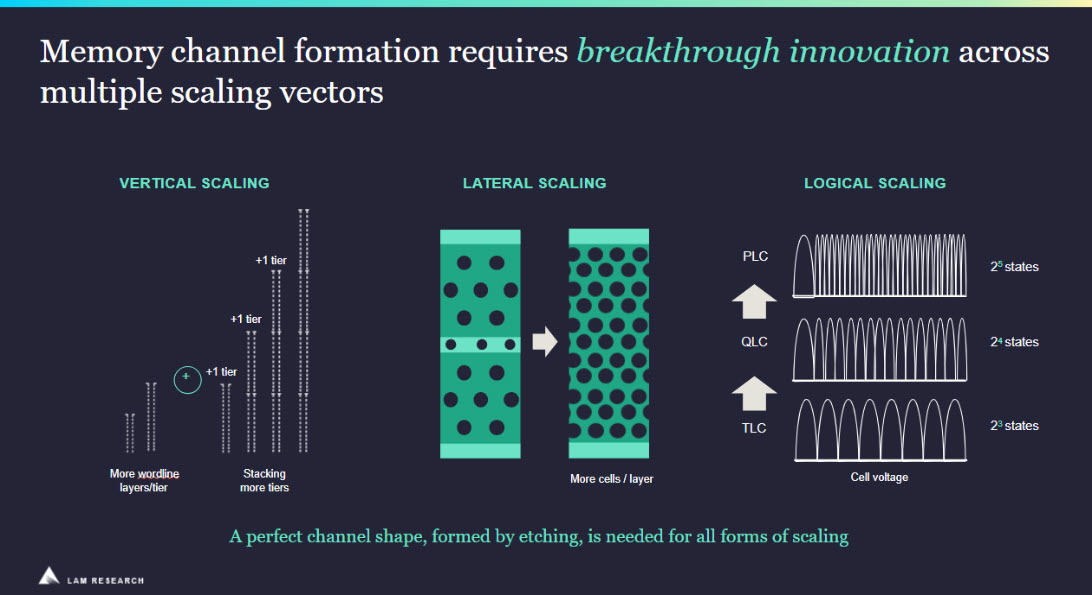
Lam Cryo 3.0 delivers:
- Industry-leading etch rates and vertical profiles for complex 3D NAND structures
- Superior process control for consistent, high-quality manufacturing
- Sustainability gains: up to 40% less energy use and up to 90% lower emissions per wafer compared to conventional etch processes*
What they’re saying: “As the industry strives to make memory smaller and taller, Lam Cryo 3.0 technology overcomes key scaling obstacles to pave the way for 1,000-layer 3D NAND,” says Tae Won Kim, corporate vice president of dielectric etch at Lam.
- “We thank SEMI for this honor and celebrate our global teams whose innovations have enabled millions of advanced NAND wafers using Lam cryogenic etch.”
Bottom line: The SEMI award highlights Lam’s commitment to delivering breakthrough solutions that accelerate our customers’ success and move the semiconductor industry forward.
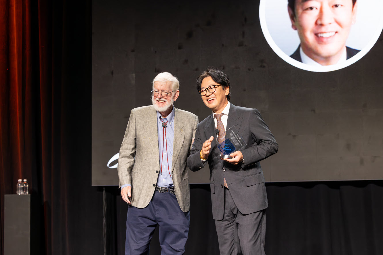
Tae Won Kim (right) accepts the award on behalf of Lam from a member of the SEMI award committee
*Based on new etch chemistries possible with Lam Cryo 3.0. 90% reduction in Kg CO2 per wafer. Estimated emissions reduction calculated using IPPC (Intergovernmental Panel on Climate Change) guidelines for greenhouse gas inventories. The estimated reduction has not been independently verified.