Lam Research Drives Technology Advancements for Next-Generation Semiconductors (SEMICON Taiwan 2022)
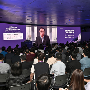

Lam’s experts were invited to SEMICON Taiwan to give keynote speeches at the MEMS & Sensor Forum, Smart Manufacturing Forum, IC Forum, and Heterogeneous Integration Global Summit. Lam was also invited to speak at the “Workforce Development Program – Women in Semiconductor (WiS) Seminar” to discuss women’s leadership in the STEM field.
Here is a recap of the main presentations from Lam Research participants at SEMICON Taiwan 2022.
Click here to see job openings at Lam
In his speech “Addressing High Volume Manufacturing Challenges and Technology Inflections in MEMS,” Dr. David Haynes, vice president of strategic marketing, Customer Support Business Group at Lam Research, said MEMS sensing devices are rapidly evolving into the new field of smart sensors.
Lam Research has formulated three strategies to help customers overcome MEMS’s high-volume manufacturing challenges:
Haynes points out that Lam Research has launched the Syndion® family of products for 300mm wafers and is developing a new generation of DSiE technology specifically for the needs of the MEMS market.
The industry is also developing a new generation of piezoelectric MEMS devices to drive the paradigm shift for MEMS devices. Since piezoelectric materials are non-volatile materials used in the etching process, they are more difficult to fabricate.
Dr. Joseph Ervin, senior director of the Semiconductor Software Products Group at Lam Research, discussed the challenges and solutions at 3nm and beyond in a presentation entitled “Using Digital Twins, Predictive Process Models and Advanced Material Engineering in Next Node Semiconductor Development.”
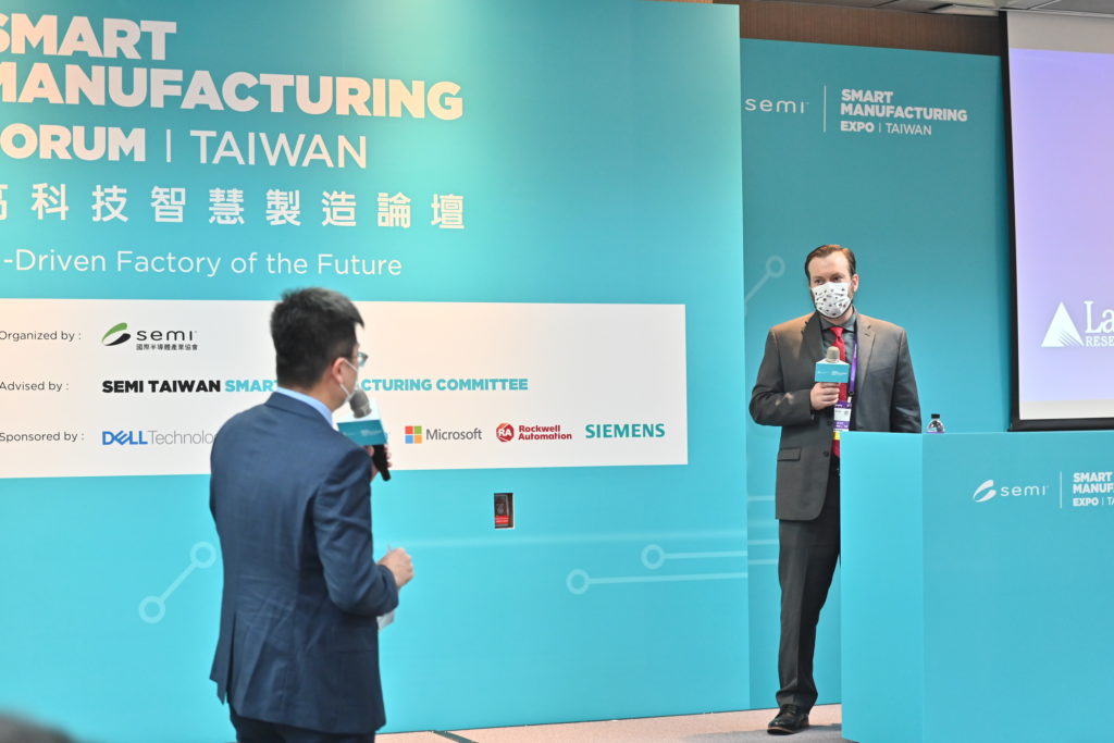
Joseph Ervin takes a question from the audience
Ervin explains that by using 193nm immersion lithography (193i) with multiple patterning, chipmakers have been able to generate advanced features down to 7nm. Using 193i lithography has become increasingly problematic at 5nm and beyond, due to the large number of patterning and process steps required at smaller feature sizes.
Unfortunately, transitioning to EUV lithographic exposure is likely insufficient on its own. 193i was a long-life lithography technology, and lithography scaling alone at 193i was not sufficient to scale logic at earlier semiconductor nodes.
Predictive process models, digital twins, automated variability control, and material optimization technologies can be used to develop next-generation devices using EUV lithography.
Click here to see job openings at Lam
Dr. Yang Pan, corporate vice president of Advanced Technology Development at Lam Research, introduced “Dry Photoresist System for EUV Patterning,” saying that Lam’s dry photoresist deposition and dry development technology is a breakthrough approach for next-generation logic and DRAM devices that is expected to help enable everything from machine learning and artificial intelligence to mobile devices.
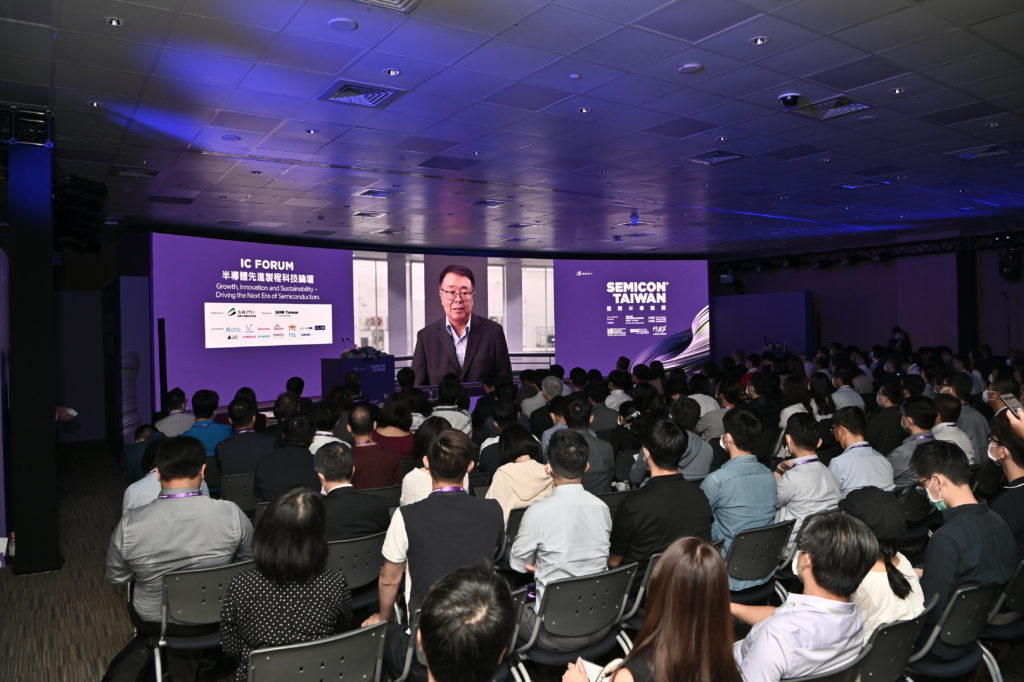
Yang Pan presented virtually
To achieve extremely low EUV patterning defects at low dose, Lam Research has engineered a holistic approach to co-optimize the complete EUV patterning flow with key differentiating steps, such as dry photoresist deposition, post-exposure bake (PEB), dry development, and pattern transfer etch.
Pan further explains that Lam’s dry EUV patterning system can be extended to define pillars and holes at pitches for future logic and memory technologies using high numerical aperture extreme ultraviolet lithography (NA EUV) technology.
In recent years, heterogeneous integration has driven packaging innovation for high-end applications like application processors (AP) and high-performance computing (HPC). These applications drive smaller features in the fan-out wafer level packaging (FO-WLP) and substrate markets. To provide better cost-effectiveness and expand the application scope of fan-out technology, fan-out panel level packaging (FO-PLP) has become another option for chipmakers.
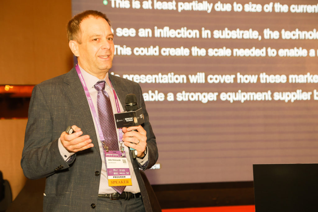
John Ostrowski talked about fan-out technology
Ostrowski says that since the low-cost fan-out process technology on panels is not mature, yields are low, which limits the FO-PLP market size. The industry has not yet invested heavily in the research and development of FO-PLP.
Ostrowski says the technical requirements for FO-PLP and substrates are converging and that the volume and growth in the substrate market is significant. The convergence of both panel markets is expected to create the volumes needed to allow more R&D investments into the panel market to help solve the key issues limiting yields.
Another issue with panel-level packaging has been the lack of standards. Traditionally many different sizes of panels have been used in the industry. That issue appears to be resolving itself. For substrates, 510mmx515mm and for FO-PLP 600mmx600mm panels are becoming the standard.
Ostrowski notes that the convergence of the technical requirements on substrates and FO-PLP will lead to the adoption of more standards. Our efforts will be around developing a common system platform to reduce costs and address challenges, including defect control, uniformity control, productivity, and cost-effectiveness.
This year’s Women in Semiconductor (WiS) Seminar was titled “Unleash the Potential of Woman Leadership.” Annie Chou, director of Spares Operation & Logistics at Lam Research, and other outstanding female executives were invited to discuss and share their experiences working in the semiconductor industry.
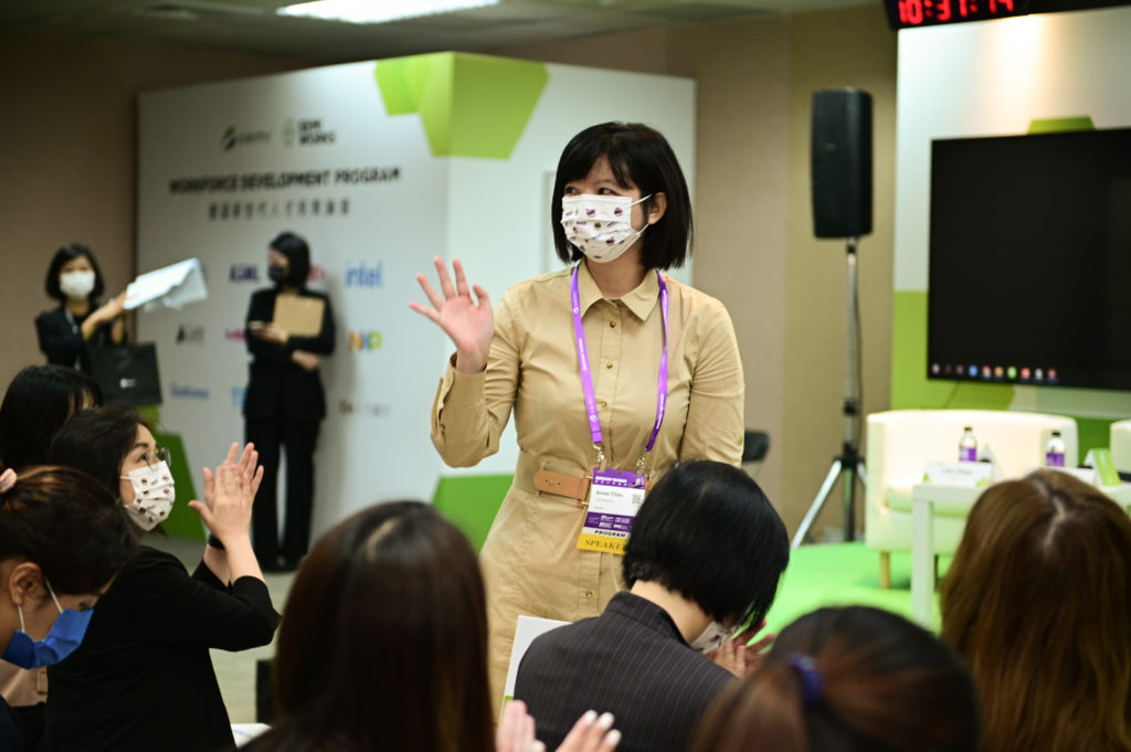
Annie Chou encouraged women to seize opportunities
Read an interview with Soon Kuek, the head of operations in Lam Malaysia and Alyson Crafton, head of the Global Information Systems’ (GIS) Common Services Organization
As the semiconductor industry continues to progress along “More Moore” to 3nm and beyond, as well as to create “More than Moore” opportunities for heterogeneous integration and special processes, Lam Research demonstrated its technological strength at SEMICON Taiwan 2022.
Lam continues to invest in advanced process development, EUV dry photoresist, high volume manufacturing of MEMS, and heterogeneous integration in response to industry trends. Lam Research will resolutely pursue innovation, push the boundaries of technological limitations, and develop solutions that keep semiconductor manufacturing moving forward.
Click here to see job openings at Lam
Frances Huang works in Communications and is based in Taiwan
This article contains forward-looking statements within the meaning of the Private Securities Litigation Reform Act of 1995. Forward-looking statements include any statements that are not statements of historical fact, including statements regarding: anticipated business results; market, industry and industry segment expectations; product development and release plans; product performance; customer and industry demand; and our ability to successfully execute business, product and growth plans or strategies. Forward-looking statements are subject to risks and uncertainties that could cause actual results to differ materially from the expectations expressed, including the risks and uncertainties described in our filings with the U.S. Securities and Exchange Commission, including specifically the Risk Factors described in our annual report on Form 10-K and quarterly reports on Form 10-Q. You should not place undue reliance on forward-looking statements. We undertake no obligation to update any forward-looking statements.