How Self-Aligned CFET Technology Could Extend CMOS Scaling Beyond 10 Angstroms

As their dimensions continue to shrink, conventional gate-all-around (GAA) nanosheet transistors may face growing challenges, such as leakage, mobility, resistance, and manufacturing variability.
A proposed self-aligned complementary field-effect transistor (SA-CFET) architecture addresses these constraints by vertically stacking N-channel metal-oxide-semiconductor (NMOS) and P-channel metal-oxide-semiconductor (PMOS) devices and using self-aligned modules to improve density and manufacturability.
What Is a CFET?
A complementary field-effect transistor (CFET) is a transistor architecture that vertically stacks NMOS and PMOS devices. This configuration can reduce cell area, increase effective channel width, and improve electrostatic control compared with side-by-side device layouts.
With SEMulator3D®, the Semiverse® Solutions team used digital twin process modeling to show that the self-aligned architecture can support static random-access memory (SRAM) and logic cells while delivering a 0.0094 μm² SRAM bit cell, a 52.7% area reduction compared with N3 technology, and at least a 10 nm overlay window across critical contact layers.
Many experts believe that the currently most-advanced transistor architecture, silicon GAA nanosheets, may begin to have physics and manufacturing issues past the 10 Å node. These challenges include:
With these challenges, it is becoming increasingly difficult to scale down the nanosheet device area or enhance device density by simply shrinking the active area, gate, or metal patterning pitch.
CFET architecture stacks PMOS and NMOS vertically to achieve significant area reduction, enhanced performance through larger effective channel width, and improved electrostatics.1,2,3,4 However, CFET architecture faces its own critical integration challenges: metal gate isolation complexity and contact crowding that can cause electrical shorts or open circuits. These issues intensify at smaller dimensions, requiring innovative solutions for scalability.
To address these challenges, we propose a SA-CFET architecture with three key self-aligned modules: SA-BPR (buried power rail), SA-CT (contacts), and SA-TSV (through-silicon via).
These process modules enlarge the edge placement error window and mitigate contact crowding, improving process margin. The architecture uses non-metal gate cut design and middle dielectric isolation (MDI) for work function split.5 SA-CFET maintains compatibility with N3 specifications (42-nm CPP, 21-nm metal pitch), transforming overlay-sensitive steps into self-aligned processes for better manufacturability.
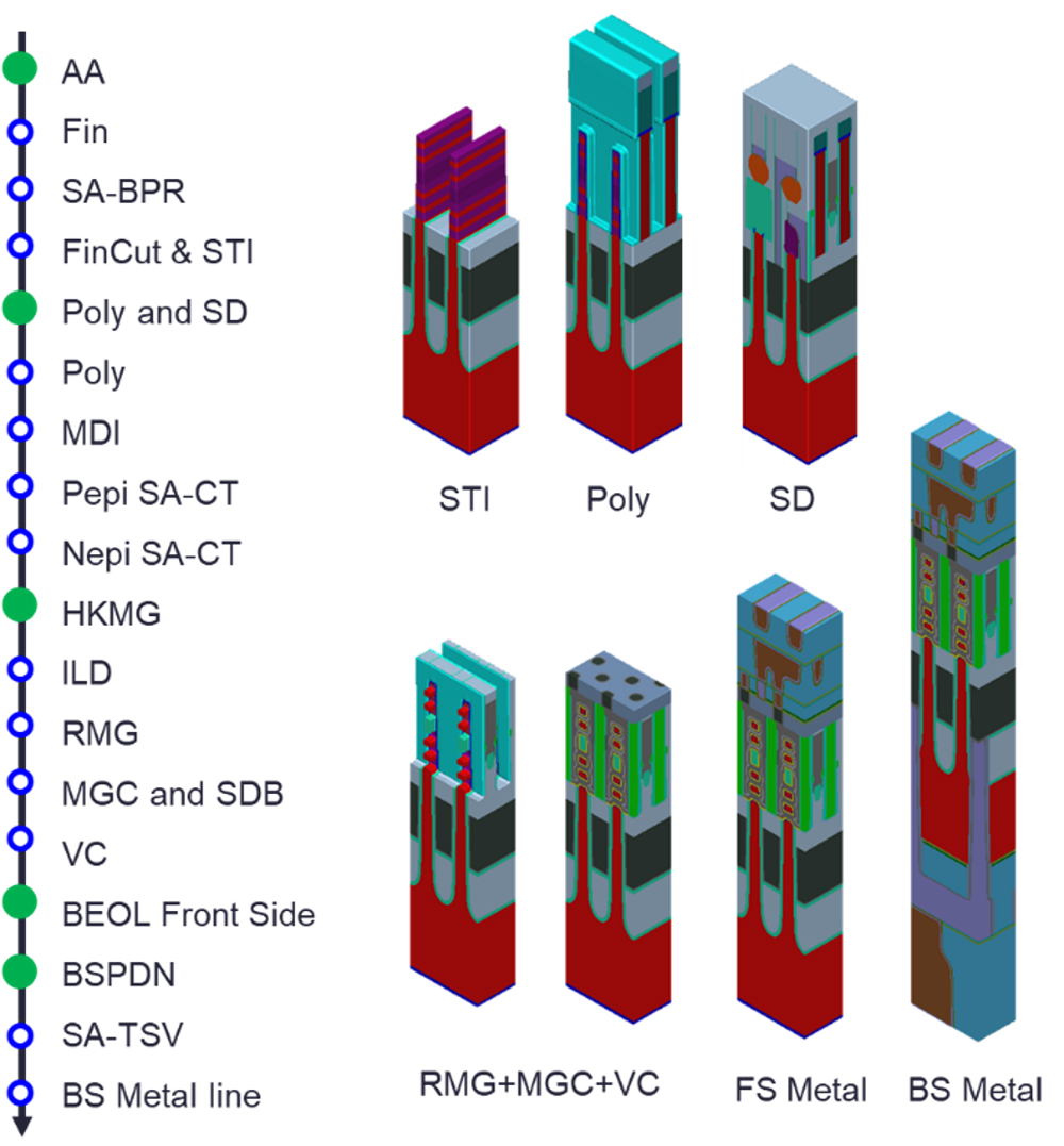
Figure 1. Key integration loops of the SA-CFET
The SA-CFET design can be used to successfully build 6T SRAM cells and logic standard cells (NOT, NAND, NOR) with no metal gate split required within any single fin, simplifying the process flow. The complete interconnection network, validated through digital twin (process) simulation, demonstrates complex routing capability while maintaining self-aligned benefits.
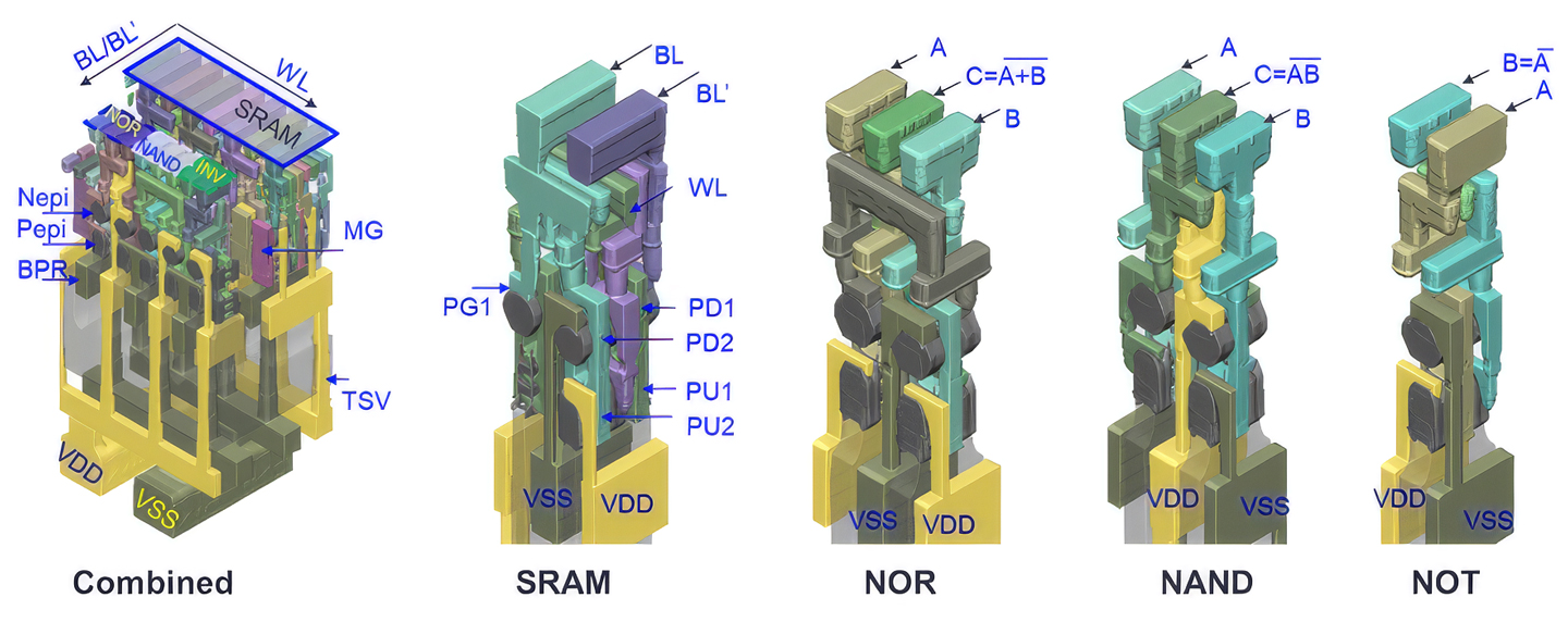
Figure 2. 3D interconnection network architecture showing SRAM and logic cells (NAND, NOR, NOT) with complex routing validated through digital twin simulation
SA-CFET achieves a 6T SRAM bit cell area of 0.0094 μm²—a 52.7% reduction versus N3 technology6 and 19% reduction versus state-of-the-art A7 CFET designs. Process robustness validation shows at least a 10-nm overlay window for all critical contact layers with no open/short failures, confirming robust process margin.
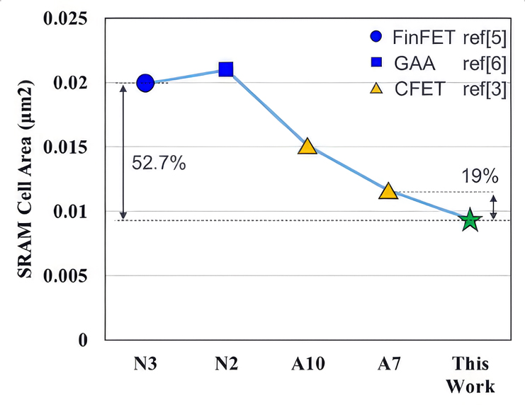
Figure 3. SRAM bit cell area comparison showing 52.7% reduction versus N3 technology

Figure 4. Overlay window validation confirming robust process margin across critical contact layers
This article describes an innovative self-aligned CFET architecture that employs multiple self-aligned processes. Using this architecture, we designed a process sequence for both a 6T SRAM device and for logic standard cells using digital twin (process) modeling.
We found the proposed architecture shares similar or even more relaxed design rules compared to current or conventional semiconductor manufacturing. It also provides an area reduction from both existing N3 devices and state-of-the-art CFET architectures.
More importantly, it avoids many of the scaling issues found in existing nanosheet architectures, achieving enhanced performance through larger effective channel width and improved electrostatics at smaller nodes. We believe that this work demonstrates a potential architectural solution to support CMOS scaling for transistors at 10 Å and beyond.