What Is Advanced Packaging? (Semi 101)

The Semi 101 series is a beginner’s guide to understanding microchips and the semiconductor industry— from components to processes to players and everything in between.

Packaging is how semiconductor chips are connected to each other, increasingly to enable high performance in a small footprint. Advanced packaging describes the many novel ways chips are built and connected to fit on smaller footprint, be higher performing, and use less energy.
Advanced packaging extends Moore’s Law by enabling more transistors on higher performing, smaller chips.

High bandwidth memory (HBM) is a prime example of advanced packaging in use today. HBM is an advanced computer memory design that plays a key role in AI by storing enormous datasets close to a graphic processing unit (GPU) for quick access.
HBM incorporates several advanced packaging techniques:
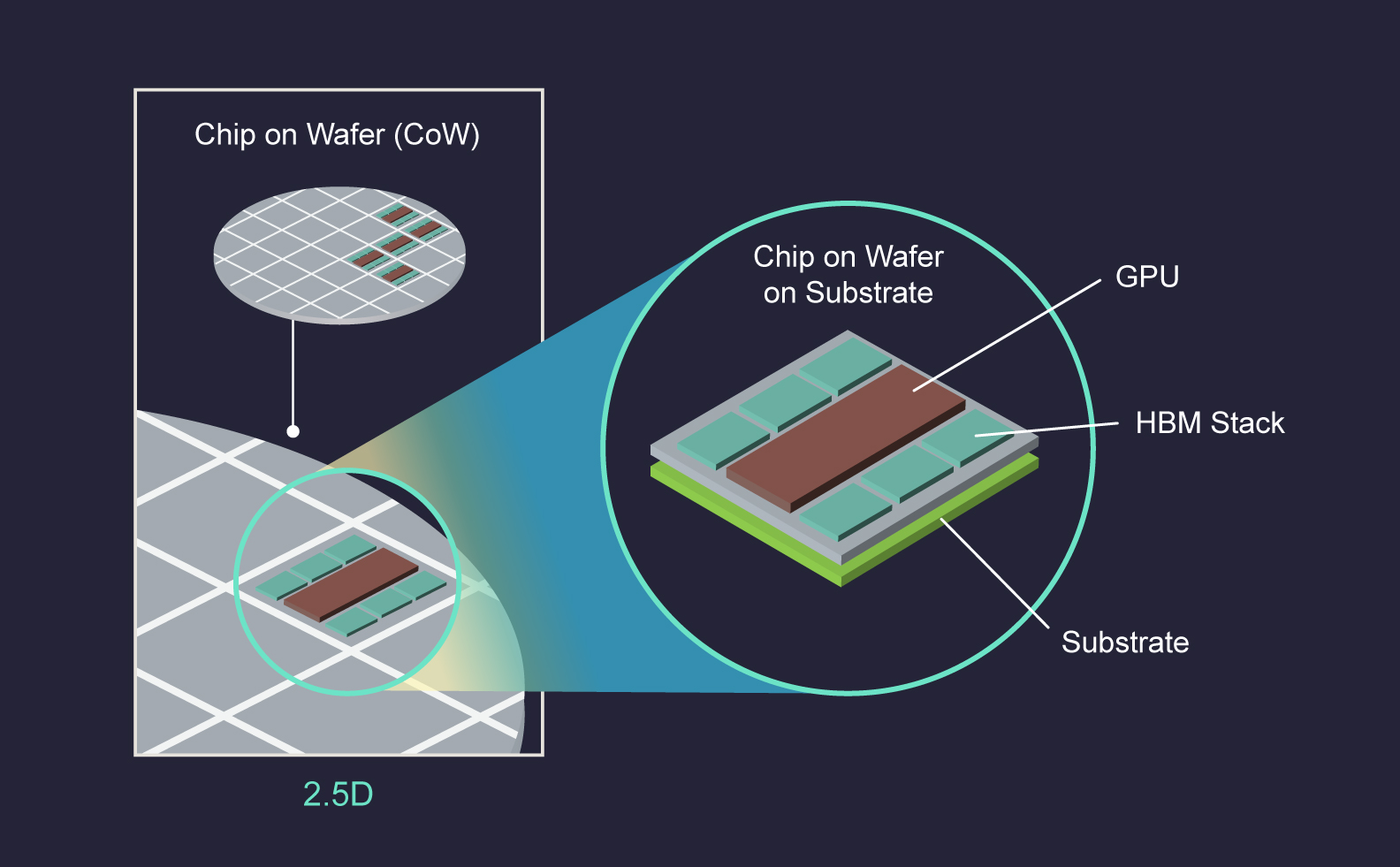
In an advanced packaging technique called “Chip on Wafer on Substrate” (CoWoS), logic (GPU) and memory (HBM) chiplets sit next to each other on a wafer, which is then cut into chips and packaged on a high-density substrate
Dig deeper: A high-density substrate is the foundational layer in advanced packaging that connects silicon dies to the printed circuit board (PCB). It routes signals, provides mechanical support, and manages heat. What makes it “high-density” is its ability to support fine-pitch interconnects, multi-layer routing, and compact form factors—all essential for modern chip architectures like 2.5D, 3D, and CoWoS.
NVIDIA's H100 AI chip is an example of CoWoS, combining one powerful GPU with six HBM stacks, each of which are formed by vertically connecting eight to 12 HBM chips. The H100 chip is considered a breakthrough for AI and is specifically designed for AI applications, particularly natural language processing and large language models.
Lam Research invests heavily in research and development (R&D) and collaborates with foundries, chip manufacturers, and consortia to develop the advanced packaging technologies that help drive the AI era.
In addition, Lam’s advanced packaging solutions are already being used by many customers today, including the following: