What Is DRAM? (Semi 101)

The Semi 101 series is a beginner’s guide to understanding microchips and the semiconductor industry – from components to processes to players and everything in between.
Dynamic random access memory (DRAM) is a type of memory that temporarily stores data that needs to be accessed quickly in a computing system, such as running applications, loading operating systems, and handling real-time tasks. DRAM has been the backbone of computing for decades, powering everything from early PCs to modern AI systems.
Unlike NAND, another type of memory device for non-volatile/long-term data storage (used in SSDs), DRAM is volatile, meaning it loses its data when your computer is turned off.
Although temporary data storage may seem undesirable, DRAM’s advantage is its simplicity. The cell structure requires only one transistor and one capacitor per bit, which allows its architecture to reach very high density.
This has allowed semiconductor manufacturers to continue scaling DRAM and keep up with the relentless demand for data speed, capacity, and efficiency.
DRAM was first invented in the late 1960s and held just a few kilobits of data, but it enabled faster and more affordable memory compared to magnetic storage.
Through the 1980s and 1990s, DRAM evolved into standardized modules—SIMMs (single in-line memory modules) and then DIMMs (dual in-line memory modules)—powering the personal computer boom.
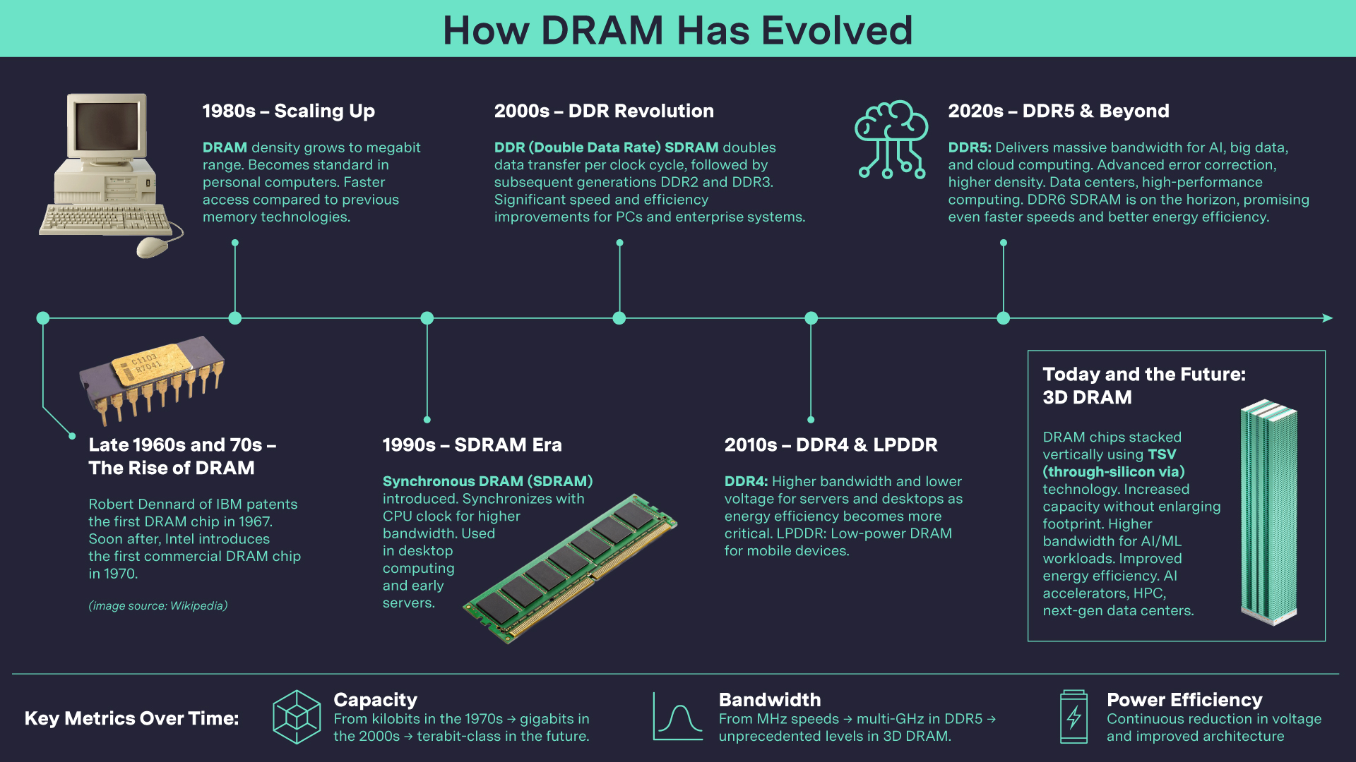
Today’s computing systems use DDR (double data rate) synchronous DRAM (SDRAM), now in its fifth generation (DDR5). DDR5 offers higher bandwidth, lower power consumption, and improved efficiency compared to previous generations (DDR1 to DDR4).
These advancements are critical for handling data-heavy workloads like AI, gaming, and cloud computing. DRAM data densities have skyrocketed—modules now store gigabytes instead of kilobits—and their data transfer speeds have reached thousands of megatransfers per second.
Most of today's DRAM (i.e., 2D DRAM) uses a planar surface design where the amount of memory cells is limited by the available surface area (length and width dimensions) of the wafer.
While chipmakers have managed to scale DRAM’s capacity for decades by moving capacitors closer together, current DRAM architecture will reach its limit, as it is becoming more difficult to scale efficiently.
Meeting increased memory demands requires denser, more complex architectures and new integration approaches.
The focus also has shifted from scaling out horizontally to scaling up vertically.
HBM incorporates specialized packaging, interconnects, and logic integration, with the benefits of:
These DRAM scaling innovations aim to reduce bottlenecks between processors and memory, enabling systems to handle massive datasets with ease.
Lam’s DRAM solutions deliver precision, uniformity, and integration excellence to meet the most demanding specs in memory manufacturing. Our products address critical challenges in patterning, etch, and deposition, enabling customers to innovate future DRAM nodes and prepare for 3D architectures with confidence.
Below are some of Lam’s portfolio of products that help customers address the most demanding aspects of DRAM scaling:
DRAM has evolved from humble beginnings into a high-speed powerhouse, and its future promises even greater performance and efficiency. As computing demands grow, DRAM will remain a critical component—continuously adapting to keep pace with innovation.
4F² is the next generation of memory cell layout (from 6F2) that packs more memory cells on a die.
DDR stands for "double data rate" and is a type of synchronous dynamic random-access memory (SDRAM) widely used in computers and other electronic devices.
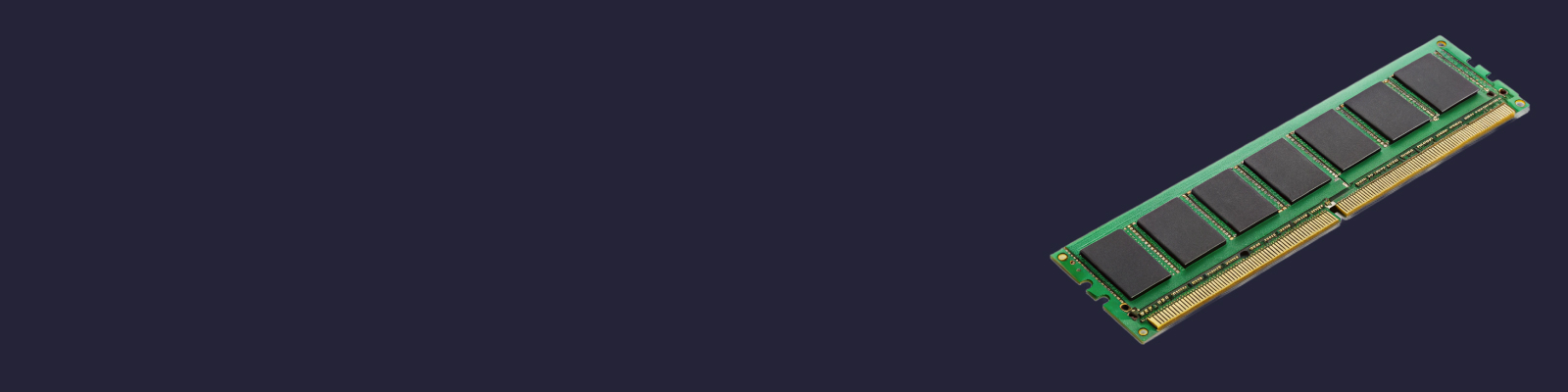
DIMMs (dual in-line memory modules) are the memory form factor that connect to the computer motherboard through a double-sided pin connection. They feature a 64-bit channel for twice the data transfer capabilities of older SIMMs (single in-line memory modules), which enable 32-bit data transfer.
DRAM (dynamic random access memory) is a type of volatile memory (needs power to retain data) that can be electrically refreshed.
HBM (high-bandwidth memory) is an advanced memory technology using 3D stacked architecture that delivers faster data access with lower energy consumption than traditional memory. Current HBM3 designs have up to 16 memory layers.
NAND is a truncated form of “NOT AND.” It’s a type of flash memory that connects transistors and is often used in memory cards, USB drives, and solid state drives.
TSVs (through-silicon vias) are tall structures between DRAM layers that create vertical electrical connections.