What Is Dry Resist? (Semi 101)

The Semi 101 series is a beginner’s guide to understanding microchips and the semiconductor industry – from components to processes to players and everything in between.

As chips become smaller and their designs more complex, the processes to create them become more challenging.
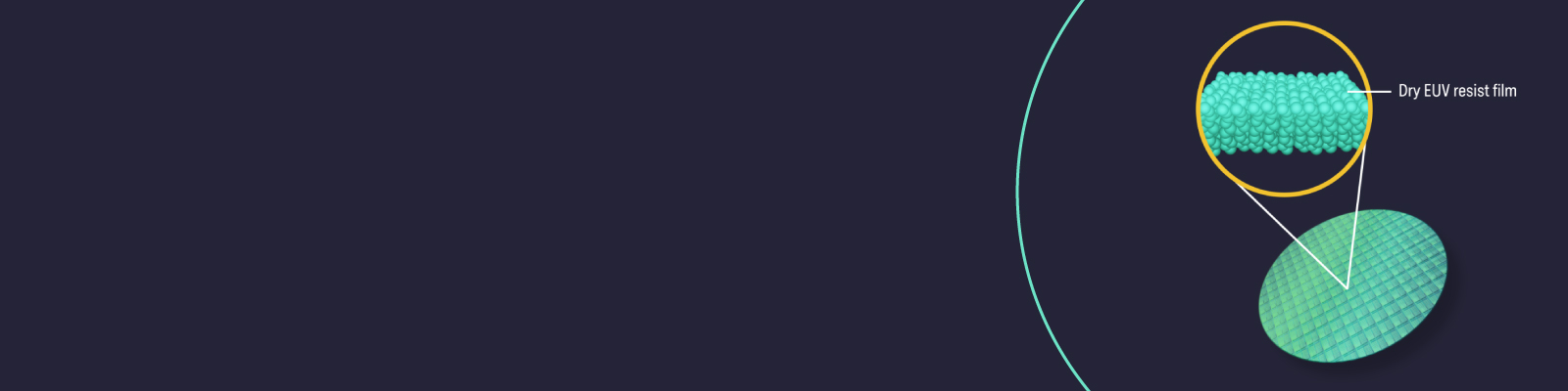
Next-generation nodes require advanced patterning that uses high numerical-aperture extreme ultraviolet (high-NA EUV) lithography and dry photoresist (“dry resist” for short) to create features that can be as small as a few nanometers wide.
Lam Research’s Aether® dry resist deposition and development process uses a series of Lam tools before and after high-NA EUV to support sub-10-nm patterning.
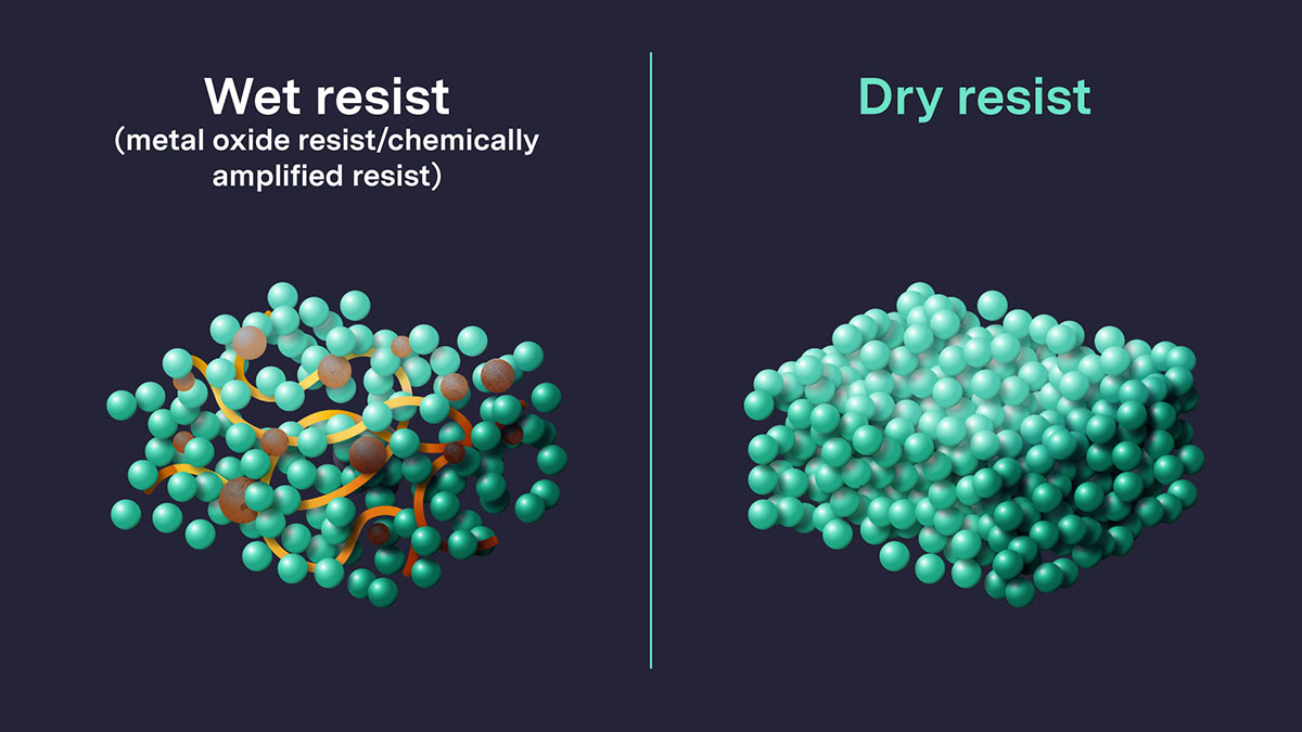
Dry resist is deposited onto a wafer using vapor phase deposition in a vacuum environment. In contrast, wet resist is dispensed in liquid form onto a wafer and then spun using centrifugal force at atmospheric pressure to spread the resist until it thins down and reaches the desired thickness.
Dry resist materials and processes are beneficial to all EUV lithography, not just high-NA, for several reasons:
Lam Research introduced its groundbreaking dry resist technology in 2020. Most recently, it launched the Aether® dry resist and development process that improves resolution, productivity, and defectivity (yield) of both low- and high-NA EUV lithography processes.
Lam Research offers dry resist tools suited for EUV lithography:
Chemically amplified resist (CAR): A type of wet resist that forms an acid during the post-exposure bake that completes the reactions started during photon exposure, significantly reducing the dose required.
Extreme ultraviolet (EUV): 13.5-nm wavelength radiation.
High-NA EUV lithography: Lithography that achieves better resolution through the use of larger EUV scanner mirrors to print smaller features and more densely packed arrays of transistors.
Lithography: Traditionally used as an artistic technique in printmaking, lithography in semiconductor manufacturing uses deep ultraviolet (DUV) and extreme ultraviolet (EUV) radiation to transfer integrated circuit device layer patterns from a reticle onto a photoresist film.
Patterning: The deposition, lithography, and etching processes involved in transferring integrated circuit features, layer by layer, from reticles into target layers on silicon wafers.
Photoresists: Photosensitive materials used to transfer integrated circuit patterns from reticles to target layers on silicon wafers. When exposed to scanner radiation (e.g., deep ultraviolet and EUV), they undergo chemical changes that delineate areas that are either removed during development or remain as a protective mask during subsequent plasma etching or ion implantation steps.
Transistor: A fundamental component in semiconductor devices used to amplify or switch electrical signals and electrical power.