Corporate VP Gowri Kamarthy Explains Akara’s Essential Role in the Era of 3D Chipmaking (Counterpoint)

Gowri Kamarthy shares what makes Akara a "once-in-a-generation" innovation for cutting-edge memory and logic architectures
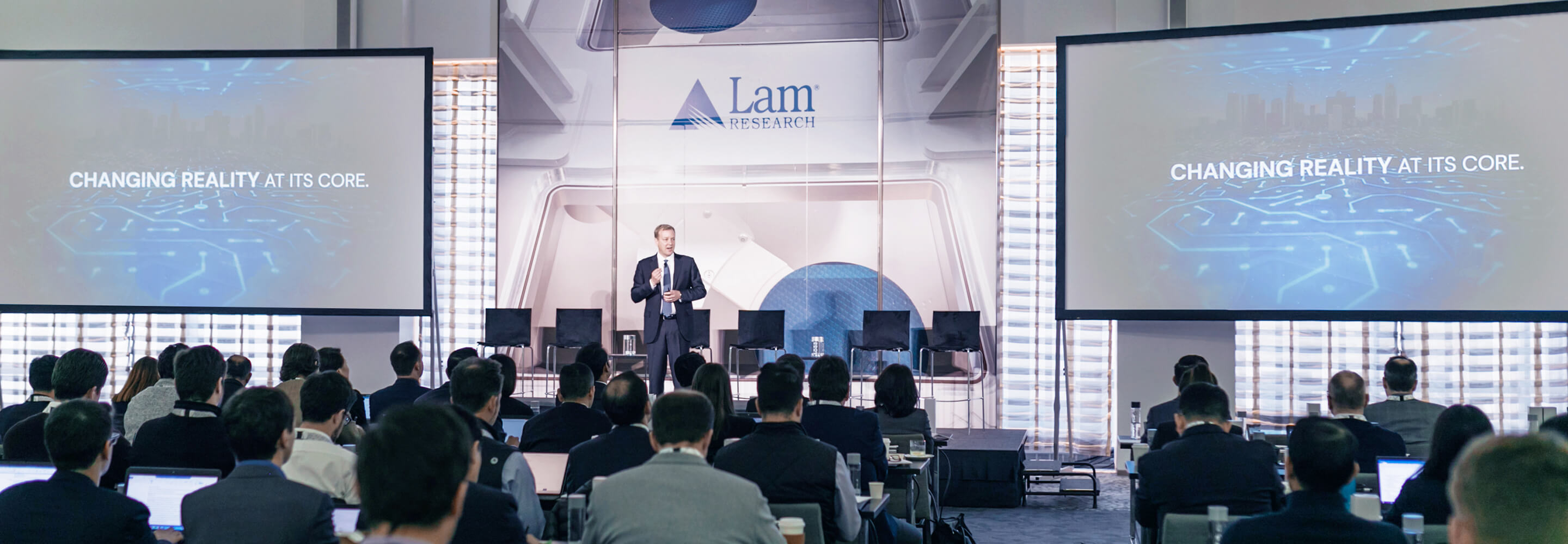
Chipmakers are turning to 3D structures for logic, memory, and storage to continue enabling Moore’s Law. But these chip architectures bring accompanying challenges, such as higher aspect ratios (i.e., the height versus the width of a device).
Gowri Kamarthy, Lam Corporate VP of Conductor Etch in the Global Products Group, spoke to Counterpoint’s Ross Young recently to discuss how Lam, and specifically, our new tool Akara, is addressing these challenges.
In the interview, Gowri shares that Akara comprises proprietary technologies to increase control and accuracy in plasma etching. These technologies include DirectDrive®, the industry’s first solid-state plasma source, which reacts to plasma condition changes 100 times faster than traditional systems, leading to significantly reduced EUV patterning defects.
In addition, TEMPO (Time and Energy Multiplexed Pulsing Operation) offers enhanced control over plasma species to maintain uniformity across complex wafer topographies. Finally, SNAP (Shaped Nanosecond Advanced Pulsing) delivers atomic-level ion energy control, enabling engineers to sculpt etch profiles with a high degree of accuracy.
Watch the video to learn more about what makes Akara a “once-in-a-generation" innovation for cutting-edge memory and logic architectures like 1,000-layer NAND, ultra-dense 4F² DRAM, and advanced GAA/CFET logic.