
- Lam Cryo™ 3.0 builds on 20 years of pioneering memory etch technology and five years of production proven cryogenic etch technologies
- The tool overcomes manufacturing challenges in scaling 3D NAND vertically, laterally, and logically
Driving the news: Today Lam announced Lam Cryo™ 3.0—an essential dielectric etch technology to produce 3D NAND devices that help enable the AI era.
- Since 2019, Lam has been the only company with cryo tools running in production for NAND manufacturing worldwide, boasting an install base of nearly 1,000 chambers.
- Our cryogenic etch technology has been proven, having been used in producing over five million wafers.
What it does: Lam’s innovative cryogenic etch technology combines industry-leading high-power pulsed plasma reactor technology, processing temperatures that can hit specific temperature targets well below -0oC, and novel etch chemistries. This combination delivers angstrom-level control of profiles and the ability to efficiently etch to new depths without compromising the feature shape.
Why it matters: Lam Cryo 3.0 is at the forefront of cryogenic etching technology, which is crucial for high aspect ratio applications and is the backbone of next-generation 3D NAND in devices, which are expected to continue to scale up to advance the AI era.
- The innovation helps maintain Lam’s position as a leader in the wafer fabrication industry while pushing the boundaries of what’s possible in memory manufacturing.
- Related: The Path to 1,000 Layers Will Be Etched
What they’re saying: “Lam Cryo 3.0 is the latest iteration in a series of memory etch technologies Lam has pioneered, going back more than 20 years,” says Sesha Varadarajan, SVP, Global Products Group. “Lam Cryo 3.0 represents a significant leap forward in cryogenic etching technology. It's a testament to Lam's commitment to forward-looking innovation, environmental responsibility, and customer success in the ever-evolving semiconductor industry.”
- “AI is driving exponential demand in capacity and on the performance of flash memory both at the cloud and the edge. This is compelling chipmakers to scale NAND flash in the race to achieve 1000-layer 3D NAND by the end of 2030,” says Neil Shah, co-founder and vice president of research at Counterpoint Research.
- “Lam Cryo 3.0 cryogenic etch technology is a significant leap beyond conventional techniques,” Shah continues. “It etches memory channels that are more than 50 times deeper than their width with near perfect precision and control, achieving a profile deviation of less than 0.1%. This breakthrough significantly enhances advanced 3D NAND yields and overall performance, enabling chipmakers well in the AI era.”
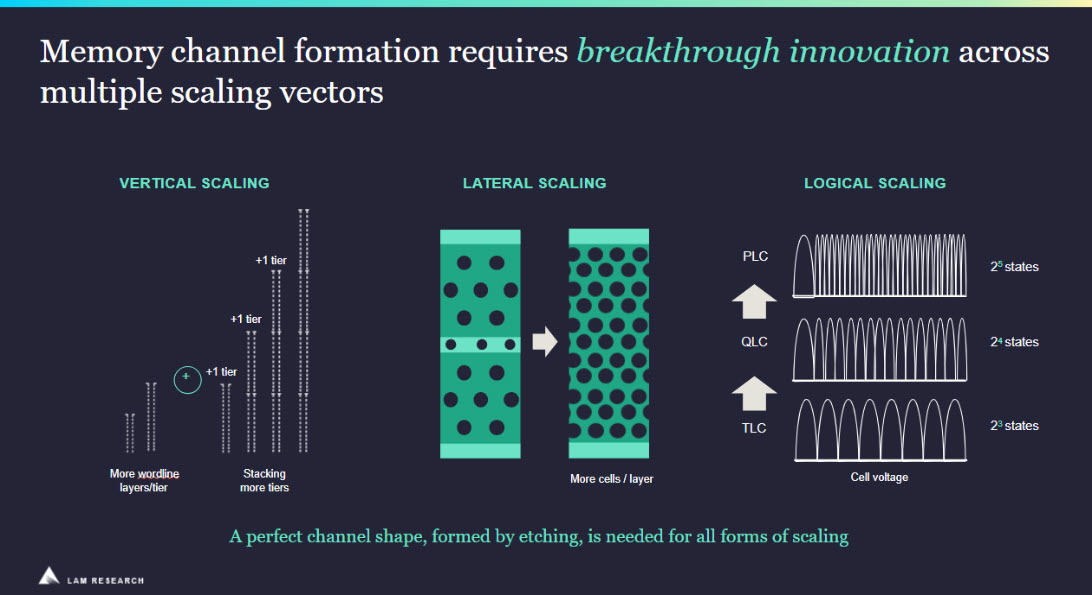
Where PLC: penta-level cell, QLC: quad-level cell, TLC: triple-level cell
Cool Technology
The benefits of Lam Cryo 3.0’s revolutionary technology are many, among them:
- Precision: With Lam Cryo 3.0, manufacturers can predictably and repeatedly etch memory channels as deep as 10 microns with less than 0.1% deviation* of the channel’s critical dimension from the top to the bottom.
- Vertical scaling: Cryo etching allows for higher aspect ratio (HAR) etches, essential for scaling to 400 layers and beyond in memory devices.
- Bit scaling and speed: Enables cost-effective bit-scaling of memory devices by providing high-yields with the fastest production etch rates. Lam Cryo 3.0 delivers etch rates two and a half times faster than conventional plasma etch technologies and at speeds two times faster than Lam’s previous-generation cryogenic etching solutions.
- Compatibility: Works seamlessly with Flex® and Vantex® etch systems, which are used by every major memory chipmaker. This compatibility ensures customers can continue to use their existing equipment while benefiting from the advancements in performance and productivity that Cryo 3.0 offers.
- Environmental benefit: Lam Cryo 3.0 has the potential to reduce carbon footprints by using process gases (and their byproducts) that have a low global warming potential. Furthermore, higher throughput results in lower system energy usage per wafer. We anticipate a 40% reduction in energy consumption per wafer** and a 90% reduction in emissions*** on cryo-enabled tools.
Big Picture
Remind me: Historically, cryo etching has been used for deep silicon etching (profile control). Recently, it has been leveraged for high aspect ratio (HAR) dielectric etching to gain one to two times increase in surface coverage that includes non-dissociated species that can be physiosorbed.
- Lam established market leadership in the etch space in 2014 by helping enable the transition from planar to 3D NAND with HAR etch solutions for memory holes.
- Five years later Lam pioneered and then perfected cryogenic memory hole etch, with the first technology used in volume production.
- Today, Lam has the only cryo tools running in production, with an install base of nearly 1,000 chambers.
Bottom line: Lam Cryo 3.0 is a transformative cryogenic etching technology for creating HAR features and scaling next-gen 3D NANDs. With etch rates more than twice as fast as conventional dielectric etching and the potential for a lower environmental impact, Lam Cryo 3.0 paves the way for customers on the path to the 1,000-layer 3D NAND that is critical to enabling the AI era.
Harmeet Singh is GVP and GM of Etch
* Profile deviation calculated by maximum critical dimension minus minimum critical dimension divided by memory channel depth.
** Estimated emissions reduction calculated using IPPC (Intergovernmental Panel on Climate Change) guidelines for greenhouse gas inventories. The estimated reduction has not been independently verified.
*** 90% reduction in Kg CO2 per wafer is based on current recipe conditions and IPCC guidelines for Global Warming Potential (GWP) calculations
Related Articles
Caution Regarding Forward-Looking Statements
Statements made in this article that are not of historical fact are forward-looking statements and are subject to the safe harbor provisions of the Private Securities Litigation Reform Act of 1995. Such forward-looking statements relate to, but are not limited to: market and industry expectations; the role and significance of our technology and products within our industry; the future success and applicability of our new technology; the future sustainability of our products; emissions and energy savings to be realized through the use of our technologies, products, and solutions; and the potential benefits of our products and new technologies. Some factors that may affect these forward-looking statements include: trade regulations, export controls, trade disputes, and other geopolitical tensions may inhibit our ability to sell our products; business, political and/or regulatory conditions in the consumer electronics industry, the semiconductor industry, and the overall economy may deteriorate or change; the actions of our customers and competitors may be inconsistent with our expectations; supply chain cost increases and other inflationary pressures have impacted and may continue to impact our profitability; supply chain disruptions or manufacturing capacity constraints may limit our ability to manufacture and sell our products; natural and human-caused disasters, disease outbreaks, war, terrorism, political or governmental unrest or instability, or other events beyond our control may impact our operations and revenue in affected areas; and technology demands and capabilities may not result in the changes that we anticipate, which are required for us to meet our future goals; as well as the other risks and uncertainties that are described in the documents filed or furnished by us with the Securities and Exchange Commission, including specifically the Risk Factors described in our annual report on Form 10-K for the fiscal year ended June 25, 2023 and our quarterly report on Form 10-Q for the fiscal quarter ended March 31, 2024. These uncertainties and changes could materially affect the forward-looking statements and cause actual results to vary from expectations in a material way. The Company undertakes no obligation to update the information or statements made in this article.