Dynamic Random Access Memory (DRAM) is the type of integrated circuit widely used today for digital electronics requiring low-cost and high-capacity memory, such as in modern computers, graphics cards, portable devices, and game consoles.
Advances in DRAM have been driven by scaling, shrinking the overall footprint as each generation progresses to the next (node to node). And so DRAM is following in the steps of NAND by evolving to three dimensions in order to build more storage (more bits) per unit area. (NAND stands for “NOT AND,” which refers to the Boolean operator or logic gate that governs the internal circuit of a NAND cell.)
- This is good for the industry because it pushes the technological envelope for memory and because increased bits per square micrometer means production costs decrease.
- Continuous scaling of DRAM technology is driving a move to 3D geometry using a stack of horizontal capacitors.
How soon do we expect the industry to evolve from 2D to 3D DRAM? Five to eight years based on current technical capabilities. Like many advancements in the semiconductor industry, the next phase begins with a plan. Or, in this case, architecture.
At Lam we’re simulating DRAM’s untested future by creating proposals for what 3D DRAM architecture could look like. We’re doing this by using our SEMulator3D® computer software, which is typically used to virtually fabricate devices by mimicking wafer fabrication. Here are some suggestions for a 3D DRAM architecture, addressing:
- Scaling issues
- Stacking challenges
- Shrinking footprints
- Innovative connections
- Via arrays
- Process requirements
Scaling Issue
DRAM is made of transistors and capacitors. A transistor carries current to enable information (the bit) to be written or read, while a capacitor is used to store the bit.
A DRAM structure is composed of a conductive material/structure called a bitline, which provides the carriers (current) to be injected into a transistor. The transistor acts as a gate that can be opened (turned on) or closed (turned off) to keep or stop the current traveling within the device. This gate state is defined by a voltage bias applied to a contact conductive structure called the wordline. If a transistor is ON, the current will flow through the transistor to reach the capacitor where it will get stored.
The capacitor has a high aspect ratio, meaning it is much taller than wide. In some earlier generations of DRAM, the capacitor’s active area used to be embedded into the silicon substrate. In the most recent generations, the capacitor is processed on top of the transistors.
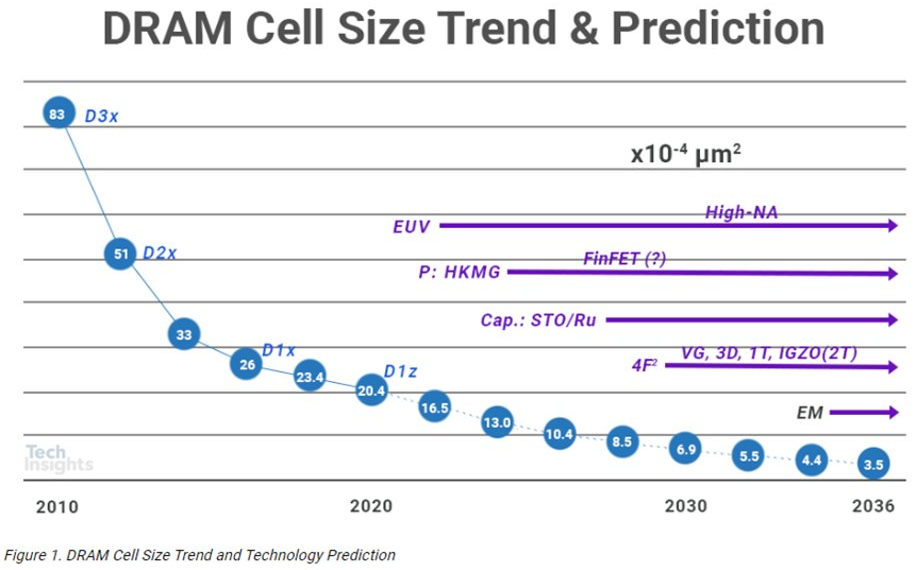
Critical to scaling is how many bits you can have in an area, or what is the average area per bit. Today (D1z on the chart above), the area per bit is at about 20.4E-4 µm2. Soon, driving higher density of bits (i.e., further reduction of the area per bit) by reducing the footprint of the capacitors by making them taller will not be possible because etch and deposition processes for capacitor fabrication cannot handle the extreme (high) aspect ratio.
On the chart above, our industry is expected to be able to maintain 2D DRAM until reaching ~10.4E-4 µm2 area per bit, which is about five years out. After that the lack of space becomes a problem that will likely demand going vertical—3D DRAM.
Stacking Challenges
A natural move to advance DRAM scaling is to put the 2D DRAM components on their side and stack them. Doing it this way presents several challenges:
- The horizontal orientation necessitates lateral etching, which is difficult because recess sizes vary greatly.
- Different materials are needed in the stack etching and filling process, making fabrication difficult.
- Integration challenges emerge when you try to connect the different 3D components.
Lastly, for this option to be competitive, capacitors need to be shortened—they can’t be as long as they are currently tall—and to be stacked to optimize the quantity of bits per unit area.
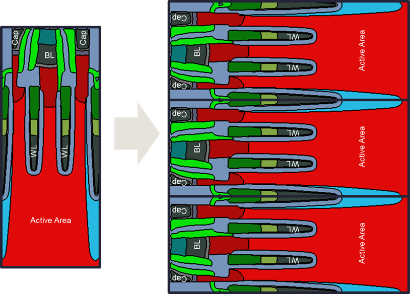
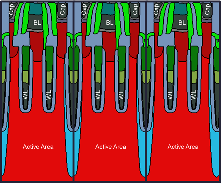
A view of 2D DRAM architecture vertically oriented (on the left). Tipping it over and stacking structures on top of each other (right) is impractical mainly because of the need for lateral cavities to be etched and filled with varying lateral depth into the Si Active Area.
Imagine the above image represents the same structure, but instead of being vertically oriented the structure is "on its back,” thereby exposing architecture to a top-down view. With this orientation nanosheets could be stacked. But, again, in this scenario the original design shows a very dense area where bitline and capacitors need to be top-down processed with high proximity. For this orientation and stacking (3D) to be achieved, the architecture needs to be redesigned.
Reimagined Architecture
Our team used Lam’s SEMulator3D to come up with several changes to provide more space for capacitor processing while reducing the silicon area, thereby shrinking the nanosheets’ footprint.
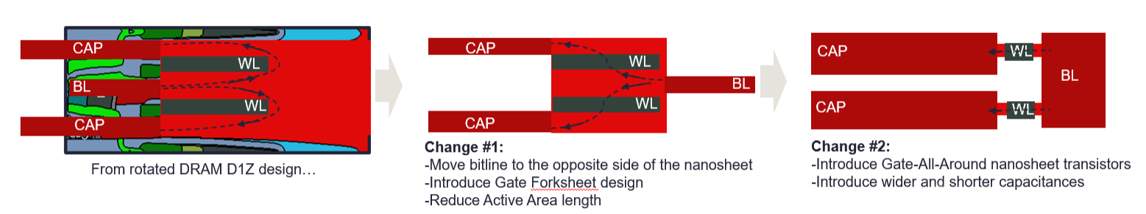
First, we moved the bitline (BL) to the opposite side of the nanosheet, so the current will travel through the entire nanosheet through the transistor gate. The effect overall increases space for capacitor processing and also reduces the silicon area’s footprint.
Second, we introduced gate-all-around transistors to further reduce the silicon active area. We also made the capacitors—once skinny and tall—short and wide. This is possible because of the space gained by moving the BL to the center of the architecture.
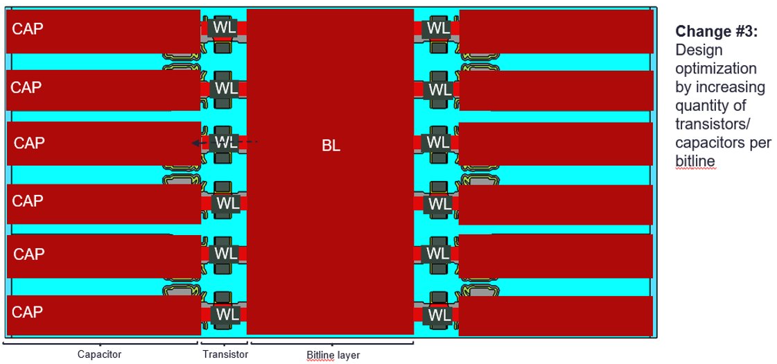
Finally, we increased the quantity of transistors/capacitors per bitline contact (no reason to be limited to two transistors per bitline) by placing transistors/capacitors on both sides of the bitline contact. This reconfigured nanosheet (as seen from a top-down view above) can then be stacked (as seen below).
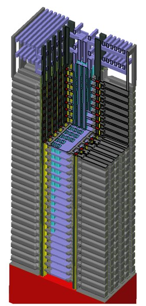
The first iteration of a stacked 3D DRAM would be 28 layers tall (above) and would be two nodes (~13E-4 µm2 per bit) ahead of D1z today. The more layers, of course, the more bits we have and therefore, the greater the density.
Innovative Connections
A new architecture for 3D DRAM is just the beginning. Along with the configuration, decisions must be made regarding metallization and connectivity.
In our design, we suggest several novel approaches to facilitate current moving through a central stack of bitlines, including an array of horizontal MIM (metal-isolator-metal) capacitors that connect each layer, as well as wrapping the gates around the silicon transistors (gate-all-around). The idea is that as a current travels, only the targeted bitlines (layers) are activated. In that activated layer current can connect to the right transistors.
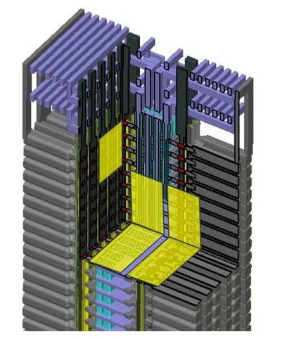
The key components of a 28-layer 3D nanosheet include:
- A stack of gate-all-around nanosheet silicon transistors
- A stack of bitline layers in between two rows of transistors
- 24 vertical wordlines
- Multibridge connections between bitline layers and transistors; transistors and capacitors
- An array of horizontal MIM (metal-isolation-mental) capacitors
Via Array
To avoid the limitations of staircase construction used in 3D NAND, we propose putting the contact inside the memory cell by introducing an array of vias that goes through the silicon stack and can stop at each level—one via per level. Once the trenches are made, we introduce an isolation spacer that’s only on the side wall.
The tall trenches are used to introduce etching medium to remove silicon and then to introduce conductive metal in the empty trenches. The result is that each square on the top (the light green and purple boxes in the last three images below) connects to only one layer below.
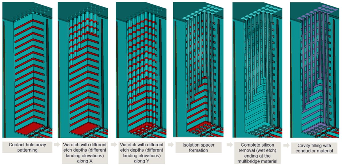
Bitline contact patterning
Process Requirements
The several modules touched on in this imaginary process require unique and innovative processes. Until now, for this type of pathfinding work, variables have been discovered and refined with physical testing. With the Semulator3D we can tweak the definitions virtually.
Our experiments result in very aggressive specifications in terms of process requirements. Etch and deposition experts may be shocked at what our simulations propose. For example, trenches with 30nm critical dimensions and 2µm depth are considered to be etched and filled in our architecture.
3D DRAM is cutting-edge design, which demands never seen or tried processes and designs. It’s the only way to move from concept to prototype. Our experiments can be pushed further to understand process variation from wafer to wafer.
Moving Forward
3D DRAM technology is expected to be the key enabler to keep driving DRAM scaling. A proper balance between the area per bit and the capacitor size (length) needs to be defined by various process/design optimization, like the ones suggested in this article.
SEMulator3D can help with fabrication by virtually prototyping new architecture designs, experimenting with different DRAM design options at different memory densities, and driving specifications for unit processes that will be needed to fabricate untested device technologies.
This work is a starting point for future technology assessment to help define detailed process and equipment specification requirements, manufacturability and yield analysis, in a way that accounts for process availability and variability, technology performance, and area and cost analysis.
Related Content
- Learn more about SEMulator3D® computer software
- Chipmaking in the Third Dimension (Lam Research)
Benjamin Vincent is director of Engineering for SEMulator3D® application in Lam’s Semiverse Solutions group