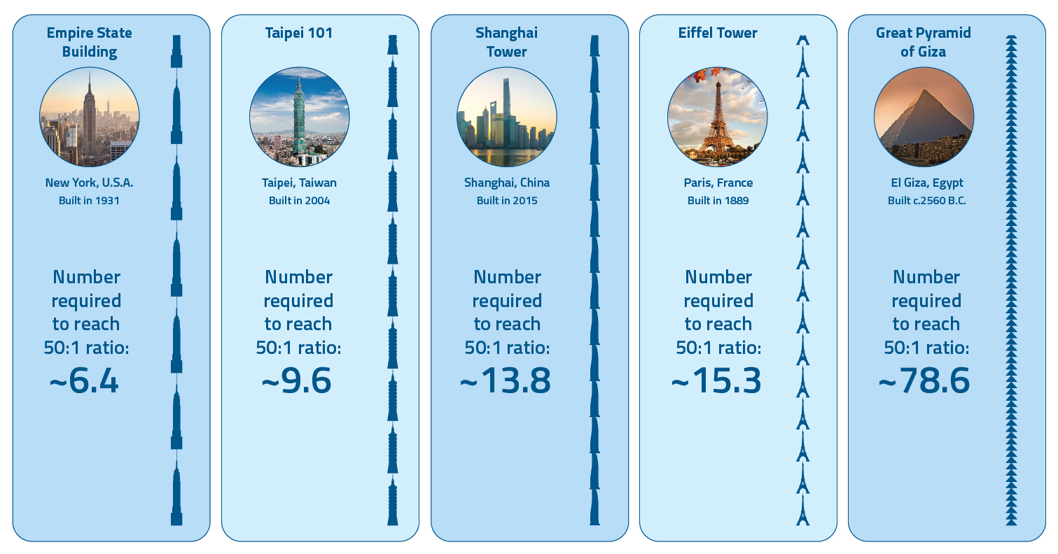
When it comes to aspect ratios – how tall an object is vs. how wide it is – even the tallest buildings in the world hardly compare to the extreme dimensions in the semiconductor industry, where aspect ratios of some device features can reach 50:1 or higher.
Already tall and narrow – or high aspect ratio (HAR) – chip structures are stretching to even more exaggerated shapes as additional device components are “squished” into smaller spaces. To illustrate this point on a larger scale, we calculated the aspect ratios of some iconic “HAR” structures and learned, for example, that a stack of ~15 Eiffel Towers would be needed to reach a 50:1 aspect ratio.
Extremely tall may be impressive, but very tall and very narrow chip features are truly remarkable. To create these challenging structures, chipmakers rely on processes like etch and deposition to deliver the atomic-scale control needed. To see additional building and other fun aspect-ratio comparisons, check out the graphics below.
Learn more about the scale of semiconductor manufacturing in our blog articles “How Big Is a Billion?” and “How Small Is Small?“


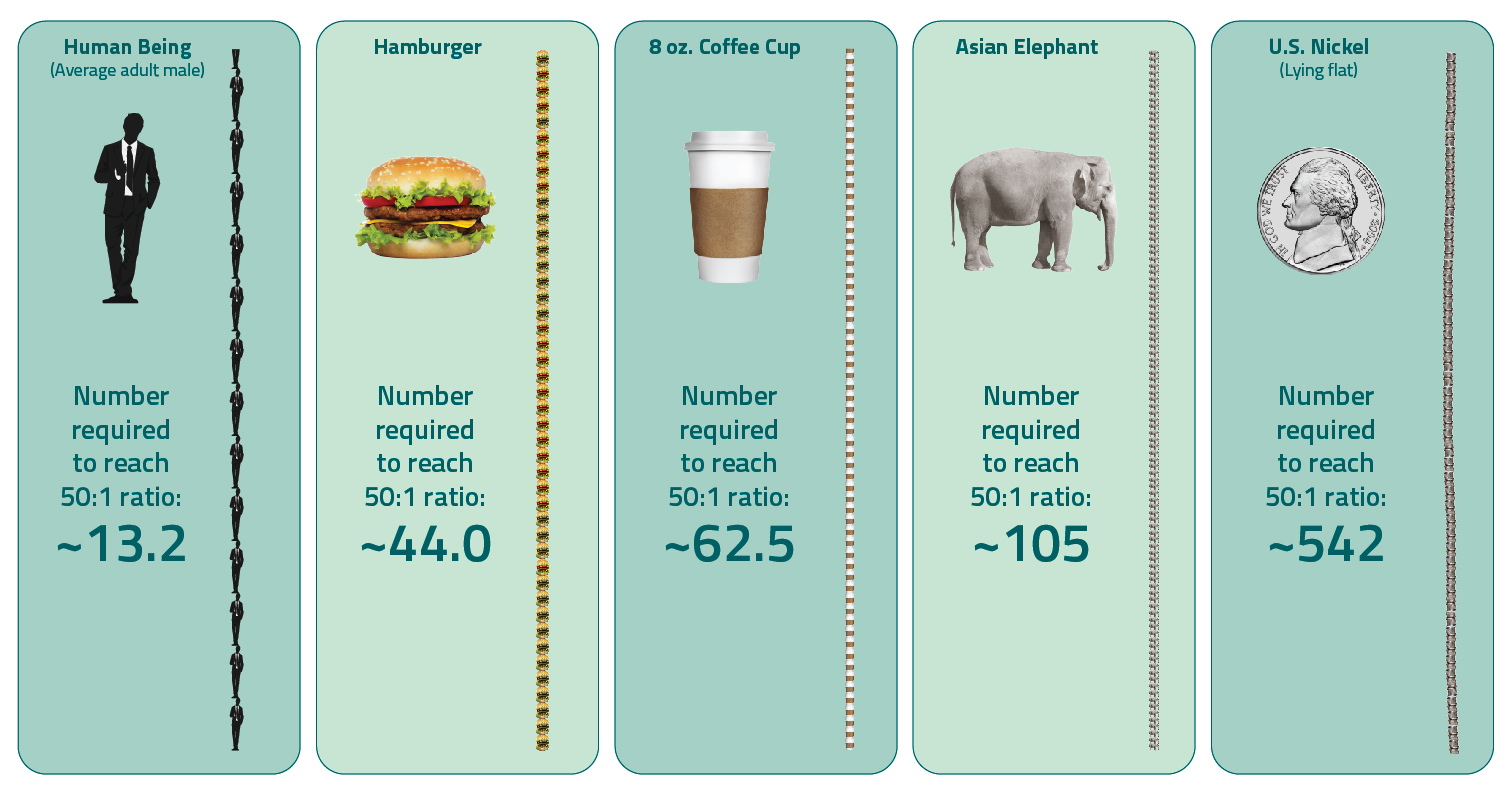
Fun aspect ratio comparisons of five objects.
Human Being (average adult male). Number required to reach 50:1 ratio: ~13.2
Hamburger. Number required to reach 50:1 ratio: ~44.0
8 oz. Coffee Cup. Number required to reach 50:1 ratio: ~62.5
Asian Elephant. Number required to reach 50:1 ratio: ~105.
U.S. Nickel, lying flat. Number required to reach 50:1 ratio: ~542.