- The semiconductor industry is searching for alternative metal line materials to replace copper due to the increasing barrier size and resistivity issues
- Ruthenium has shown promise as a potential replacement, outperforming copper and cobalt at smaller dimensions
The semiconductor industry has been diligently searching for alternative metal line materials to replace the conventional copper dual damascene scheme, because as interconnect dimensions shrink, the barrier accounts for an increasing fraction of the total line volume.
The barrier layer's dimensions cannot be scaled down as much as the metal line width (Fig. 1). Popular barrier materials such as TaN (tantalum nitride) have high resistivity and exhibit more electron scattering at the sidewalls. Therefore, the increase in the relative barrier size causes a more significant RC delay, which may reduce circuit performance and increase power consumption.
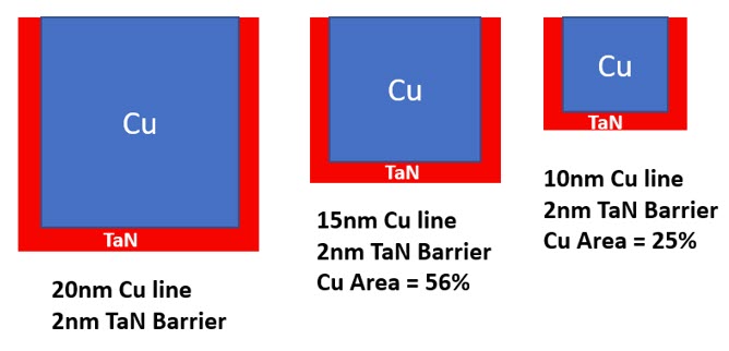
Fig. 1: Image of Scaling in Copper and Barrier Line Structure
Recently, new alternative metal lines such as Ru (ruthenium) and Co (cobalt) have been suggested and tested.1 These materials can mitigate resistivity issues at narrow line widths and smaller areas.2 Process modeling can be used to benchmark the performance of Ru, Co, and other metals, such as Cu (copper), in a damascene vehicle with varying critical dimensions (CDs), for different trench depths and sidewall angles (Fig. 2). Average line resistance, two-line mutual capacitance, and RC values can be extracted for the total conductor cross-sectional area using modeling. Then, trends can be compared between the proposed Ru, Co, and Cu metal schemes.
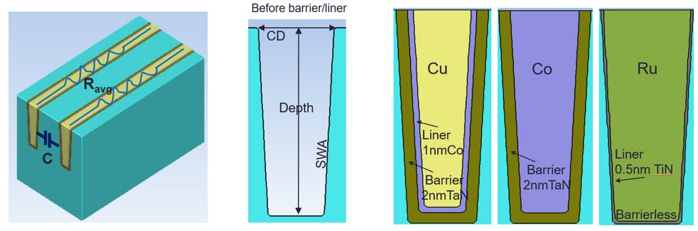
Fig. 2: 3D structure of two metal lines for R and C extractions (left) and 3 cases with different metal and barrier materials (right).
To systematically investigate the design and material impact of using these different metals, a Design of Experiments containing 1,000 virtual split experiments was executed using a Monte Carlo uniform distribution across three variables (CD, depth, and sidewall angle).
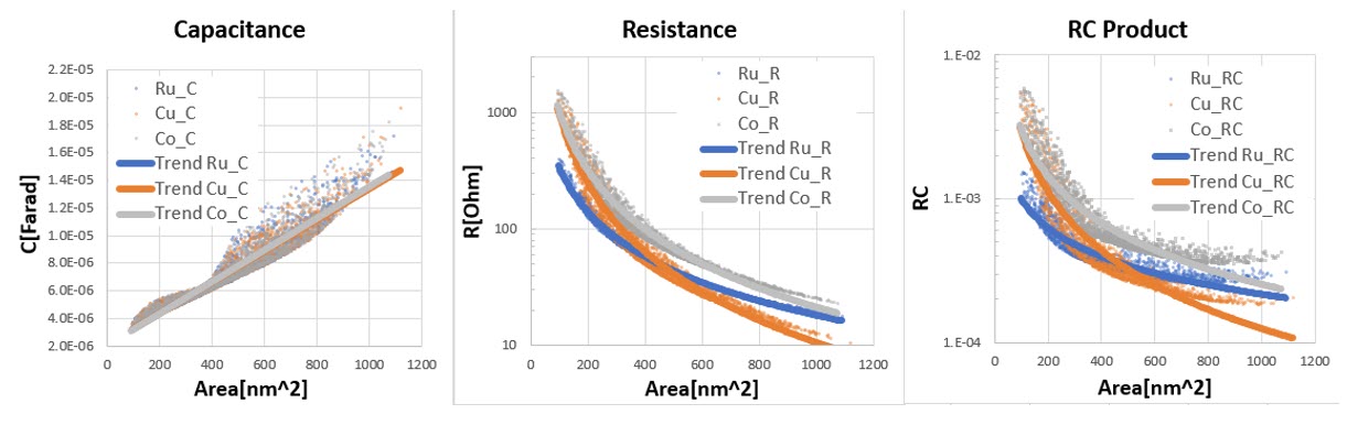
Fig. 3: RC DoE results (dots: DoE data, line: trend curve). From left to right: Capacitance vs. Area, Resistance vs. Area, RC vs. Area.
Figure 3 highlights crossing points for R (resistance) and RC (resistance capacitance) for each metal, demonstrating that the barrier-less Ru scheme outperforms the other two metal materials at smaller dimensions. This occurs at a line CD value of ~20 nm and an area value at ~400 nm2, respectively. The results indicate that the barrierless Ru line resistance is lowest at a line CD < ~20 nm. At line CD values less than 20 nm, resistivity of the 2 nm TaN barrier dominates the resistance of the Cu and Co lines, causing a sharp resistance increase. Additional scattering at the wall and grain boundaries also occurs as the line CD shrinks, which contributes to higher resistance. Trench etch depth and sidewall angle appear to change resistance linearly. Resistance is reversely proportional to the line’s cross-sectional area.
Impact of line edge roughness (LER) on resistance was also investigated.
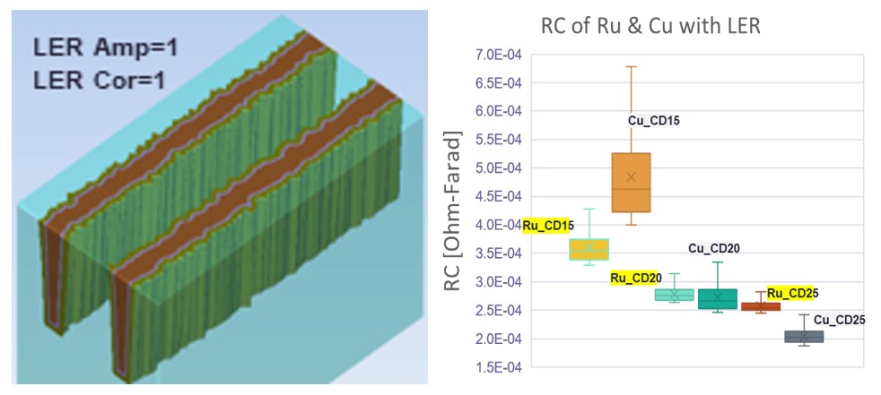
Fig. 4: (a) Cu line model view with CD=20 nm when LER Amplitude =1 and Correlation = 1 (b) Box plot of DoE results for Ru and Cu lines (CD=15,20,25 nm cases)
In Fig 4(b), due to the barrierless structure, the Ru line’s RC values (at a line CD of 15 nm) shows far less sensitivity to LER amplitude than Cu, whereas Cu is very vulnerable to RC value changes due to the highly resistive TaN barrier.
In conclusion, traditional scaling requires a 2-3 nm minimum barrier/liner thickness, leaving little space for Cu lines at modern advanced logic nodes. New metals, such as barrier-less Ru, are being considered as a potential replacement for Cu while maintaining the ability to satisfy electromagnetic reliability requirements.
This study indicates that Ru may be a superior metal candidate at advanced nodes, with much lower RC delay. Typically, many wafer-based experiments would be required to perform this type of metal scheme pathfinding. Virtual semiconductor process modeling is an alternative method to investigate metal line design options at a much lower time and cost.
REFERENCES
1. Liang Gong Wen et al., "Ruthenium metallization for advanced interconnects," 2016 IEEE International Interconnect Technology Conference / Advanced Metallization Conference (IITC/AMC), San Jose, CA, USA, 2016, pp. 34-36, doi: 10.1109/IITC-AMC.2016.7507651.
2. M. H. van der Veen et al., "Damascene Benchmark of Ru, Co and Cu in Scaled Dimensions," 2018 IEEE International Interconnect Technology Conference (IITC), Santa Clara, CA, USA, 2018, pp. 172-174, doi: 10.1109/IITC.2018.8430407
Daebin Yim is a senior manager, Semiconductor Process & Integration Engineering