As integrated circuit designers bring more sophisticated chip functionality into smaller spaces, heterogeneous integration, including 3D stacking of devices, becomes an increasingly useful and cost-effective way of mixing and connecting various functional technologies. One of the heterogeneous integration platforms gaining increased acceptance is high density fan-out wafer-level packaging (FOWLP). Primary advantages for this packaging solution include substrate-less package, lower thermal resistance, and enhanced electrical performance. It is an example of more-than-Moore processing, where technologies other than pure Moore’s Law scaling help to provide greater integration and favorable economics.
Heterogeneous Integration Techniques
High-density fan-out packaging has gained traction for addressing the form factor and performance requirements for mobile phone packaging. Key building blocks for this technology include redistribution layer (RDL) metal and megapillar plating. Redistribution layers are used to route the high-density connections on the silicon chip to the lower density connections of the printed circuit board. Multiple layers of RDLs are required in order to enable signal routing to the board.
As shown in Figure 1, megapillars are the vertical metal connections that connect the levels. Solder bumps from the top die are positioned on the megapillars, and the connection is completed using solder reflow.
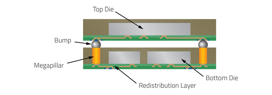
Figure 1. Interposer structure in 2.5D packaging.
Megapillar Process Challenges
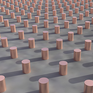
Megapillars are distinguished by their size: they are typically about five times as tall and wide as more standard copper pillars. A traditional approach to building them would be to use conventional electroplating. This is a long and slow process, but the biggest issue is that this process commonly yields unacceptably non-uniform results. Electroplated megapillars will vary in height with the local current loading density, and some level of doming or dishing may result on the tops of the mega-pillars rather than producing the desired flat surface (Figure 2). The height and feature-shape non-uniformities can result in the need for an additional subsequent planarization steps (e.g., CMP), unreliable connections that will degrade device performance, increased overall processing time, and higher cost.
The die-layout variations that impact these electroplating results include the feature shapes, widths, and aspect ratios as well as the thickness of the surrounding photoresist and the feature density in a given region. The distance across which these differences may evolve can be the wafer, a die, or between individual features.
One way of attempting to solve this would be to plate excess metal over the targeted thickness and then to reverse the plating polarization and current. This will etch back the added metal in order to narrow the height distribution or leave the tops of the megapillar flatter. But this approach may not be effective in improving uniformity across the various length scales, and often leads to poor morphology, yielding rough mega-pillar surfaces with pitting and edge corrosion.
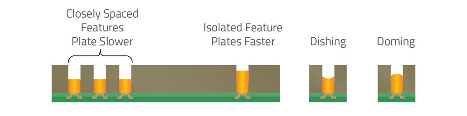
Figure 2. Some of the common variations observed when electroplating megapillars, including loading issues, dishing, and doming.
Lam Solution
Lam addresses this issue with a proprietary process called Durendal®. It yields high-quality, smooth surfaces at the tops of the megapillars and uniform megapillar height across the wafer. The entire Durendal® process can be performed on the SABRE® 3D tool.
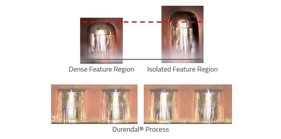
Figure 3. Uniform, high quality mega-pillars obtained in SABRE® 3D using Durendal® process. The bottom image compares mega-pillar height at the wafer edge (left) and wafer center (right).
The Durendal® process provides an economically efficient means of die stacking in a manner that gives good yields and solid, reliable connections. We expect that, in the future, the Durendal® process will be an important contributor to the increased adoption of FOWLP as a packaging technique for die stacking.