As DRAM technology nodes have scaled down, access transistor issues have been highlighted due to weak gate controllability. Saddle Fins with Buried Channel Array Transistors (BCAT) have subsequently been introduced to increase channel length, prevent short channel effects, and increase data retention times [1]. However, at technology nodes beyond 20nm, securing sufficient device performance (such as retention time and drive controllability) have become more challenging. Therefore, DRAM manufacturers have been looking for methods to improve device performance using BCATs without modifying their existing DRAM device schematics. To improve the performance of DRAM Saddle Fins, virtual process modeling can be used to study fin structure effects and develop optimal fin structures.
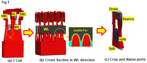
Fig 1(a) displays a single cell of a conventional DRAM that consists of 2 Word Lines (WLs), a Bit Line (BL) and 2 Storage Node Contacts (SNC). The Saddle Fin is produced during the WL etch step (prior to WL metal deposition) and is located below the cell wordline (Figure 1(b), inside the yellow dotted circle). The Saddle Fin structure can be seen in detail by making a vertical cut in the wordline direction (Fig.1(b)). During device simulation, the Saddle Fin performance can be measured by virtually cropping a transistor and adding ports at the Gate, Source and Drain after an SNC Process (Fig.1(c)).

Figure 1 displays a single cell of a conventional DRAM that consists of 2 Word Lines (WLs), a Bit Line (BL) and 2 Storage Node Contacts (SNC) in Figure 1(a). There are 3 images in the figure. The Saddle Fin is produced during the WL etch step (prior to WL metal deposition) and is located below the cell wordline (Figure 1(b), right center inside a yellow dotted circle). The Saddle Fin structure can be seen in detail by making a vertical cut in the wordline direction (Fig.1(b), right). During device simulation, the Saddle Fin performance can be measured by virtually cropping a transistor and adding ports at the Gate, Source and Drain after an SNC Process (Fig.1(c), showing the gate, source and drain).
During simulation, we can also look at the important process parameters that affect fin structures & device performance. In our study, only the fin structure itself (including the fin height & fin curvature) will be optimized under the assumption that the active area (AA) and WL CD should be fixed in the Saddle Fin design scheme.
As shown in Figure 2, fin height is most affected by the silicon/oxide etch ratio. Fin curvature is affected by the silicon fin sputter etch ratio & sputter etch angle during the WL etch step. The range of each of these input parameters needs to be set prior to performing a linear regression of device performance under a uniform Monte Carlo simulation. The SEMulator3D Analytics module can be used to locate the significant input parameters for each metrology target, and build a regression model for each selected target using these significant input parameters.

Figure 2 displays an image that describes the fin height, sputter angle and sputter ratio of a Saddle Fin. There is also a table displayed in this image that describe the fin height and fin curvature ranges for the process parameters used in our experiment. The Silicon/Oxide etch ratio ranges for our study are shown, with values between 0.8 to 1.5. The Silicon Fin Sputter Etch Ratio is also displayed, with values between 0.5 and 3. Finally, the Silicon Etch Sputter Angle is displayed, with values between 40 – 60 degrees.
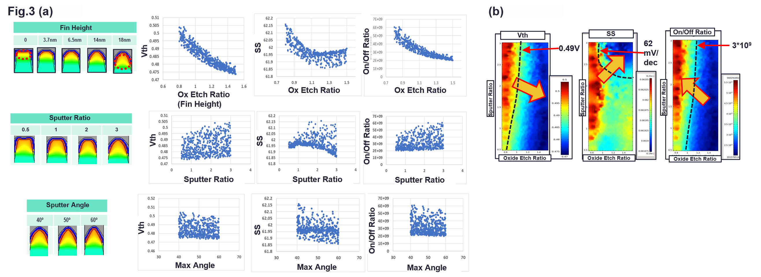
After regression analysis, we can identify statistically significant process parameters using a sensitivity analysis. Once these process parameters that significantly affect performance are identified, it is easy to optimize various parameter settings in a pre-selected process window simply by looking at the simulated relationship between the process parameters and the metrology targets. An example of typical results can be seen in Figure 3(a). For example, in our fin height DOE, as Fin height increases, Vth decreases, but the on/off ratio also decreases because Ioff increases. This means that the fin height should be optimized by considering the trade-off between Vth and the On/Off ratio (Off current). Fig.3 (b) displays contour maps which are useful for concurrently seeing the relationship between two process parameters and any selected metrology target. Using the sensitivity analysis and linear regression capabilities in SEMulator3D, we can determine the optimal process parameter range. For example, if we wanted Vth <0.49V, SS <62mV/dec, Ion/Ioff >3*109, the optimal process conditions are to have an Oxide Etch ratio between 1.0 – 1.2, a sputter ratio >2, and a max angle >50.

Figure 3 displays results of a simulation, with a group of 9 significant process parameters tested for sensitivity. Scatter plots are shown for each parameter on one axis, with a metrology target shown on the opposite axis, with simulation results displayed in Figure 3(a) on the left. One the right side of the image, we display contour maps which are useful for concurrently seeing the relationship between two process parameters and any selected metrology target.
These types of studies can be used to determine the optimal fin height and fin curvature which would produce the best device performance. The results from these studies can be employed to develop a high-performance saddle fin profile for current or next generation DRAM products.
Reference
[1] C. M. Yang, C. K. Wei and C. S. Lai, IEEE Transactions on Device and Materials Reliability, vol. 16, no. 4, pp. 685-687, Dec 2016