
Every few months, new and improved electronics are introduced. They’re typically smaller, smarter, faster, have more bandwidth, are more power-efficient, etc. – all thanks to a new generation of advanced chips and processors.
Our digital society has come to expect this steady drip of new devices as sure as the sun will rise tomorrow. Behind the scenes, however, engineers are working feverishly on semiconductor roadmaps, ensuring that the next-generation chips needed to power them will be ready. For a long time, chip advancements have been achieved by shrinking the size of transistors so that more could be fabricated on a wafer, thereby doubling the number of transistors every 12-24 months – what is commonly known as Moore’s Law. Over the years, significant innovations were needed to keep pace, including copper/low-k interconnects, new transistor materials, multiple patterning schemes, and three-dimensional (3D) architectures.
The shift to developing 3D structures introduced new challenges, which are intensifying as aspect ratios increase. As you might imagine, 3D requires radical changes in the way devices are designed, necessitating new materials and new deposition and etch approaches to make the vision a reality. In this article, we will explore some of the significant milestones the semiconductor industry has overcome in its journey to 3D.
Setting the stage: planar processing
Creating integrated circuits began as a two-dimensional problem: take a flat sheet of silicon, place various structures across the surface, connect them with wires. This was accomplished by depositing layers of material, patterning them using photolithography, and etching into the exposed areas to create the necessary features. It was an enormous breakthrough for the electronics industry.
As technology requirements continued to evolve, more circuitry needed to be built in ever tighter spaces to support smaller structures. What used to be a relatively straightforward process became increasingly complex.
As the cost of creating 2D structures continued to mount and viable approaches for scaling in the two-dimensional plane were exhausted, 3D structures became more attractive. The semiconductor industry began developing early selective etch applications that could support 3D well over a decade ago and they have continued to expand, from packaging to non-volatile memory – even to the transistor itself.

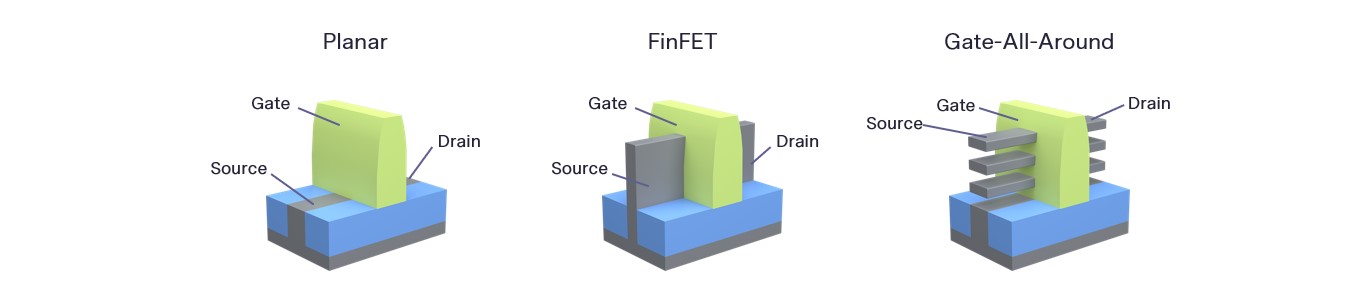
Transistors move to 3D
The workhorse of many electronics system is the transistor. Historically, transistors have been flat structures whose characteristics were decided by how wide and long the transistor channel was. Control of the transistor’s behavior came from a gate placed over the channel. This provided only so much control, since the other sides and bottom of the channel were not controlled.
The first move from planar came by creating a fin for the channel that could be controlled by the gate on three sides. However, access to all four sides of the transistor is needed for optimal control, which is now driving the move to gate-all-around (GAA) transistors. In GAA structures, multiple wires or sheets are stacked on top of each other, with gate material fully surrounding the channels.
Flash memory moves upward
The shift to the third dimension was applied to NAND flash memory a decade ago, when previously horizontal strings of memory bits were stacked upward.
The vertical arrangement consists of alternating thin layers of materials and the process stacks as many layers as possible. It requires incredibly careful manufacturing in at least two respects: first, each layer must be uniform in thickness and perfectly flat so that each bit in a layer is of the same dimensions as every other bit; second, the layers must be interconnected. This is accomplished by first building a layer stack and etching to drill holes all the way through the stack, then filling those holes with the proper connection materials. Both are extremely challenging etch and deposition tasks that require precision execution.
These challenges limit how many layers can be in a stack, and new approaches will be needed to increase layer count.

Looking ahead: 3D DRAM
Dynamic random access memory (DRAM) relies on a completely different physical mechanism than 3D NAND, requiring an altogether different approach.
DRAM needs tall capacitors, which can be a challenge to build precisely in a 2D array. Stacking them vertically is even harder, and more development is needed to find economical ways of layering dielectrics and active silicon in a stack. Lithography may need to affect multiple layers at once – a high-volume process is not yet available.
3D packaging adoption continues to gain traction
Chips are packaged for placement on printed circuit boards (PCBs). Historically, a package was simply a way to protect a delicate silicon chip and supply a way to connect it to the board. Today, packages often hold multiple chips and a need to shrink their footprint has pushed them into 3D.
3D packaging requires that chips be stacked, which involves making densely packed connections between chips – connections that can improve signal speeds because they are both much shorter and can transfer more signals at the same time. In a stack of more than two chips, however, some of those signals need to move through conduction channels to connect to a chip higher up the stack; these channels are known as “through-silicon vias” (TSVs).

Notable end market applications for 3D chip stacking have been in memory – high-bandwidth memory (HBM) being the most visible example. It’s also possible to stack a memory chip onto a CPU or other logic chip, making the process of fetching data from memory much faster.
3D is now essential to scaling
It is now standard practice to consider 3D when addressing all scaling limitations in semiconductor manufacturing. Although 3D may not be an option for solving every problem, it has been particularly useful in the applications described above.
With each new application comes the question of how it can be built, requiring innovative thinking and continuous development in silicon processing that positions semiconductor manufacturing equipment as a primary enabler of the chip industry’s inflection to 3D.