- Semiconductor manufacturers scale new heights as they embrace vertical integration
- Lam’s Metior succeeds where optical measuring falls short
In their ongoing effort to pack more computing power into less space, chip manufacturers are adopting scaling approaches that extend designs and stack components vertically—a major shift from the drive to shrink features horizontally that has dominated the industry for decades. This is especially true for memory devices like 3D NAND. To ensure the performance of these vertical designs, the dimensions of the thick film stacks and the high aspect ratio (tall and narrow) features must be tightly controlled, which requires precise measurement.
Optically based measurement technologies are challenged by these new applications for a couple of reasons. For one, increases in absorption and dispersion degrade optical signals. Also, complex structures that are less accessible to direct visibility require complicated modeling to generate results.
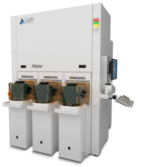
Metior®, Lam’s mass metrology tool, measures thick film stacks, high aspect ratio structures, and buried (hidden) etched features— critical components that enable vertical scaling of the next generation of microchips—faster and more precisely than optical measurement. It can help engineers produce new 3D architectures with higher process yields and less time and money spent on measurement.
Mass Metrology
Mass metrology can measure changes down to the angstrom (Å) level. An Å is a tenth of a nanometer, roughly half the diameter of a single silicon atom. That is about a millionth of the thickness of a human hair!
The foundation of Lam’s Metior mass metrology lies in the simplicity of the measurement. It derives changes in mass directly from changes in weight and converts to thickness based on the known density of the material and the area covered by the film. No modeling. No complex calculations.
Metior’s ability to measure mass changes with a precision of 30 µg equivalent to a change of 1.8Å for a silicon layer on a 300mm wafer. Importantly, Metior’s sensitivity does not change with layer thickness so that its relative sensitivity (% change in thickness—a parameter often measured for process control) improves for thicker films.
Metior measures mass changes with a precision of 30 µg, equivalent to a change of 1.8Å for a silicon layer on a 300mm wafer.
The advantages of Metior mass metrology are many:
- Measurement precision does not depend on layer thickness, composition, transparency/opacity, or any other material characteristic.
- Conversion from mass to thickness depends only on material’s density.
- Precision stays constant so that relative sensitivity to changes in thickness actually improves for thicker stacks and taller, narrower features.
- It is non-destructive, enabling direct measurement on product wafers. No sampling. No blanket films or test wafers. No waste.
- It works with any material —essentially all semiconductor materials—and a single measurement recipe covers all use-cases.
- No complicated interpretations. No arbitrary conversions (loading factors). No modeling. No complex calculations.
3D NAND
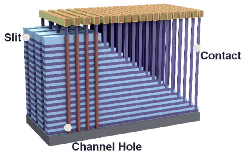
3D NAND memory is an extreme example of vertical integration. The memory matrix, which in conventional designs is a two-dimensional horizontal array, becomes a three-dimensional array with memory strings arranged along vertical channel holes.
- The device includes multilayered stacks of alternating films (usually oxide and nitride—ONON). Rows of vertical channels are separated by deep (high aspect ratio) slits. Contacts, which provide communication to the outside world, also begin as deep narrow holes etched into the device which are then filled with conductive material.
- All these features contain multilayered liners and fills.
Thick Stacks
3D-NAND memory devices incorporate thick, many-layered ONON stacks. Current generation devices use 176 ON pairs, and the next generation will go to 232 pairs.
- In a >17X pair class device, the full stack deposition adds about 1g of mass to a 300mm wafer, giving Metior mass metrology a 0.003% sensitivity (1g/30µg)
- At 2XX pair class device, the mass of the full stack mass grows to about 1.3g improving Metior’s relative thickness sensitivity to 0.0023% (1.3g/30µg)
HAR Etching
Stack deposition is followed by etching to form various high aspect ratio (HAR) trenches and holes, which are often hidden and difficult to measure. Mass metrology monitors and controls HAR etch processes by:
- Determining the time required to complete the etch process: Process development engineers monitor material removal over repeated etch cycles on a single wafer to determine removal rates and process endpoints.
- Detecting instances of incomplete etch processes: Process engineers monitor change in mass of the etch.
- Providing feed forward control: Mass measurements made after film deposition allow process engineers to tune subsequent etch process time.
Liner Deposition
In 3D NAND, the memory channels are lined and filled with concentric layers of various materials. The diameter and profile of the channel and the thickness of the liners are critical for proper device functionality.
- The diameters of the tops of the channels are easily seen and measured but the cross-sectional profile, bottom diameter, and thicknesses of liner and fill materials are difficult to measure, especially using traditional methods.
Most of the liner mass is deposited on the vertical channel walls, which multiplies the sensitivity of the mass metrology measurement—a small change in liner thickness causes a large change in mass. Mass monitoring of liner deposition processes can help process engineers by:
- Yielding reliable information about the profile and bottom diameter by combining optical measurements of top channel diameter with mass measurements of deposition thickness in a hybrid approach.
- Detecting variations in deposition rate for different wafers and feeding information forward. Wafers are processed in batches and variations in the temperature within the furnace, where liner materials are deposited, may cause variations in the deposition rate for different wafers—sometimes as much as 20%
- Matching etch and deposition rates among single-wafer process chambers.
Other Applications
Other applications of mass metrology in semiconductor manufacturing processes include:
- Isotropic etch processes create complex, buried, hidden structures. Measuring mass changes enables captive control of isotropic etch process (correlating to initial material deposition) and direct process recipe tuning.
- Baking, annealing, plasma treatment, UV curing typically do not cause visible changes in the material. They do cause changes that can be monitored with mass measurements.
- Oxidation occurs whenever wafers are exposed to air. Mass metrology has been used to investigate changes caused by differences in e queue time as wafers wait for processing.
- Voids can occur in many materials. They can be detected with mass metrology, and the information used to decide whether to pass, reprocess, or scrap the wafer.
- Ion Implant: Non-linearities and discontinuities in thermal wave measurements create difficulties in its use to monitor ion implant processes. Mass metrology measurements are linear and continuous.
The applications mentioned for the Lam Metior mass metrology technique are applicable for many technologies including logic, memory, power devices, and CMOS image sensors. Metior provides precise, reliable, high-throughput inline monitoring and control of film thickness, etch-rate, and other critical parameters across a wide variety of wafer-processes. Its ability to measure thicker film stacks, higher aspect ratio structures, and buried (hidden) etched features will be increasingly valuable as the industry continues to scale vertically
Hendrik Hans is a business development director in CSBG