Abstract: In this article, we demonstrate a pathfinding technique for a novel Vertical DRAM technology. First, we identify important process parameters (defined by current semiconductor production equipment capabilities) that strongly impact yield. By using a virtual model, we then perform experimental optimization of the Vertical DRAM device across specific target ranges, to help predict and improve the yield of this next generation product.
Introduction
Process and device technologies have had to overcome numerous technical challenges as DRAM memory devices have transitioned between different cell architectures. When DRAM technology nodes went beyond 20nm, limitations of current Buried Channel Array Transistors (BCAT) architectures started to occur. 3D structures, such as Transistor Saddle Fins, have been introduced to increase channel length, prevent short channel effects, and increase data retention times [1]. Saddle Fin based architectures have good performance but are also known to be sensitive to process variations. Row hammer, which happens when there is leakage between adjacent memory cells, has become a challenging problem due to the increase in DRAM cell density [2].
Due to these issues, many DRAM manufacturers are now making efforts to identify alternatives to current DRAM architectures. New device architectures such as 3D DRAM, Vertical DRAM and others are also being explored. Manufacturers generally prefer to use the same materials used in their existing DRAM devices when developing a new DRAM device architecture, since it can be disruptive to fab operations to use new materials on existing Fab equipment.
Virtual process modeling with Coventor SEMulator3D® can help engineers with process pathfinding of new DRAM architectures. During this pathfinding process, exploration of potential systematic and parasitic defects can be explored. In this article, we will demonstrate how virtual fabrication can be used to explore semiconductor process sensitivity in a Vertical DRAM architecture.
Background and Experimental Studies
The conventional manufacturing sequence used to build a Vertical DRAM is depicted in Fig. 2. After well and channel doping, the Si vertical channel is etched using a Self-Aligned Double Patterning (SADP) process to create the cross-line patterns in the X and Y directions. A replacement gate nitride spacer is then deposited to protect the Si sidewall from source-drain (S/D) ion implantation. Doping profile calibration is made using Monte Carlo ion implantation, with a diffusion process based upon the surrounding structures. Next, buried bitlines (BLs) are fabricated using a deep Si etch process followed by an STI gap fill process for electrical isolation of the BLs. After the replacement gate nitride is removed, a gate oxide is deposited. The wordlines (WLs) are formed using a damascene patterning or direct metal etch process. Finally, cell capacitors are formed after a WL gap fill CMP process to expose the silicon and the storage node contact.
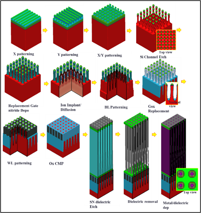
Figure 1: Vertical DRAM process flow
Fig. 2(a) shows the values of VTH (threshold voltage) and SS (subthreshold swing) at various Si pillar diameters. Both VTH and SS increase as Si pillar diameter increases due to the “floating body effect (FBE)”. The FBE is due to accumulation of holes in the vertical Si pillar body that are generated in the junction region. This phenomenon can cause off-state leakage and loss of information from the memory cells, and is the same effect seen in partially depleted-silicon on insulator (PD-SOI) structures. As the DRAM Si pillar diameter decreases, leakage current (Ioff) decreases (Fig. 2(b)). This is a similar effect that one would see in a fully depleted body where FBE effects are completely removed, such as those visible in a fully depleted silicon on insulator (FD-SOI) device [3].
However, VTH also decreases as the Si pillar height decreases due to short channel effects. Short channel effects occur when the channel length is comparable to the depletion layer widths of the source and drain. If the channel length decreases, depletion regions at the source & drain overlap the channel, and the barrier to electron injection from the source to the channel is decreased. Lowering this barrier lowers the effective VTH. The results of short channel defects are demonstrated in Fig. 3. In our 3D model shown in Fig. 3(a), we see a decreased pillar height at the cell edge. This decreased height is caused by insufficient etching due to the “pattern loading” effect present during the channel etch process. Pattern loading occurs when pattern density, pattern configuration, aspect ratio, and other variations cause etch or deposition differences across different portions of a die. In our example, the decreased pillar height at the cell edge causes a lower VTH at the cell edge than at the cell center, due to a
reduced channel length (see Fig. 3(b))
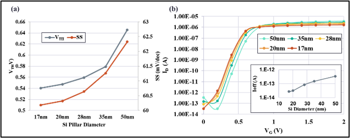
Fig. 2 (a) VTH and SS of Vertical Transistor as a function of Si Pillar diameter; (b) ID-VG curves and Ioff values at various channel widths
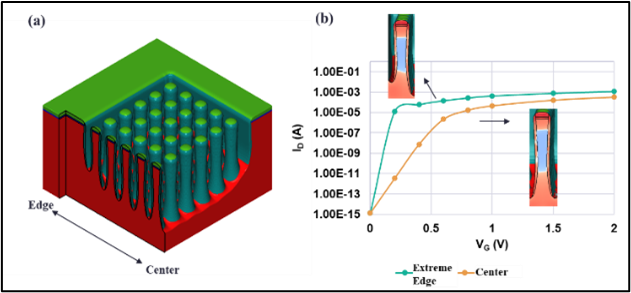
Fig. 3 (a) Varying Si pillar etch depths between the cell center and edge due to a pattern loading effect; (b) ID-VG curves at the cell center and extreme cell edge
We can perform process window optimization to satisfy both cell center and cell edge process constraints using each of our 5 significant process parameters. We identify important process parameters by executing a linear regression. These parameters include the spacer oxide deposition thickness in the x/y direction, etch depth and angular sigma during the Si pillar etch process, and gate oxide deposition thickness. We can use our current manufacturing process capabilities (mean value and standard deviation for each process parameter) to identify the optimal process conditions that will allow us to meet our specified target performance. In this case, we want to stay within ranges of both VTH (0.48V - 0.53V) and SS (58-64mV/dec) at both the cell center and the edge area. As shown in Table 1, we can increase the “inspec %” (the success rate of staying within our VTH and SS target ranges) from 1% to 67.6%, by changing the original (nominal) process values of our selected process parameters to optimized mean values. We can further increase the inspec% to 81%, by reducing the standard deviation (or variability) of Si pillar etch and spacer thickness during X/Y SADP patterning (Table 1 and Fig. 4). Improved yield can be reached by re-targeting process step settings (mean values) and controlling the standard deviation of specific process steps. The VTH gap between the cell center and the cell edge is reduced after retargeting from 0.053V to 0.042V using current etch capabilities. To further reduce the VTH gap between the cell center and edge, one could increase the Si pillar etch depth. The Si pillar etch depth is the most significant parameter affecting VTH. At the cell edge, this requires a suppression of pattern loading effects through improved etch process capabilities. In real life terms, this requires not only greater process control during the dielectric deposition process but also during the Si pillar etch process when fabricating the Vertical DRAM structure.
Table I New mean and standard deviation for inspec% maximization by process window optimization
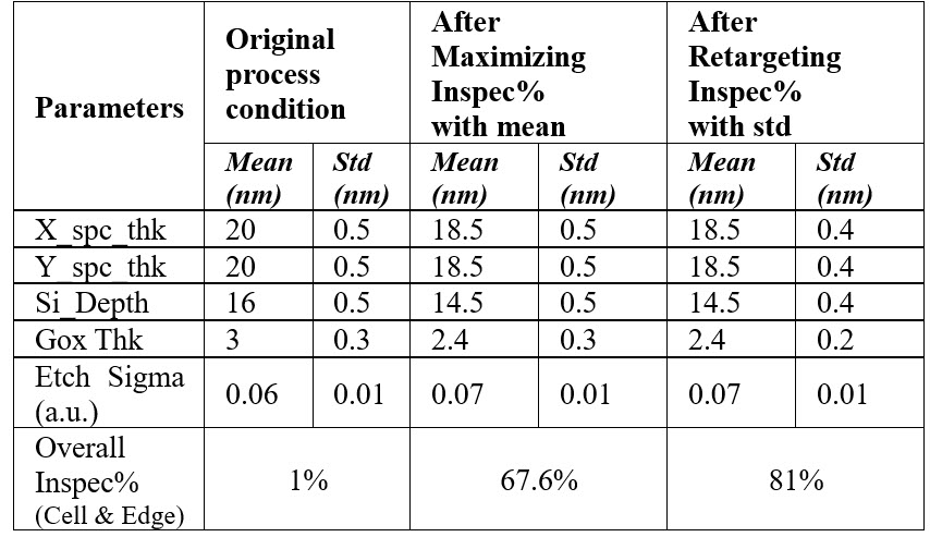
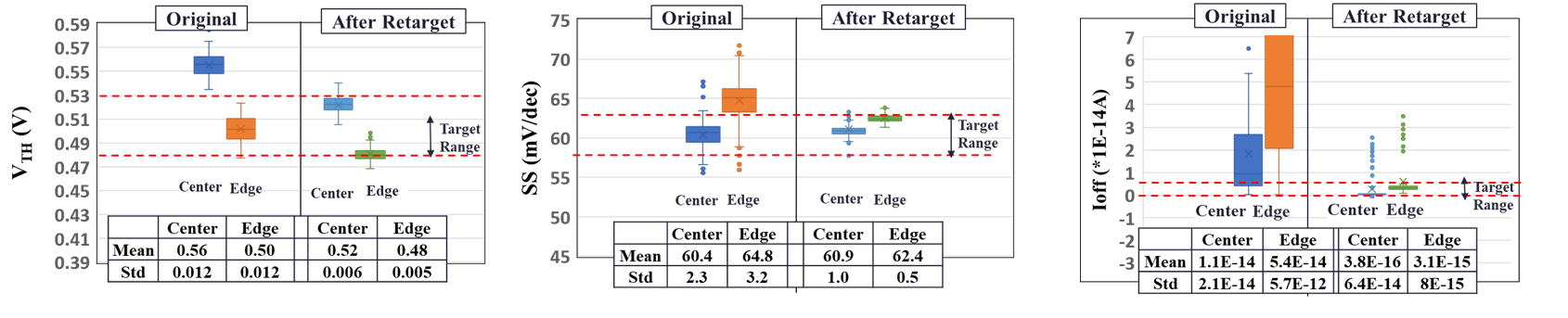
Fig. 4 VTH/SS box plot at cell center and cell edge displaying the initial and retargeted process conditions, respectively
Conclusions
In this study, we demonstrated a technique to provide guidance for manufacturing a new Vertical DRAM device. Using virtual fabrication, we were able to identify some important process parameters that contribute to parasitic defects in a Vertical DRAM and explored the effect of process variability on device performance at both the cell center and the cell edge. Using this technique, engineers can predict and improve the yield for a new device structure (such as this Vertical DRAM) using existing process manufacturing limitations, prior to performing costly wafer-based experimentation.
TaeYeon (TY) Oh is a semiconductor process and integration engineer, Semiverse Solutions
References
1. C. M. Yang, C. K. Wei and C. S. Lai, IEEE Transactions on Device and Materials Reliability, vol. 16, no. 4, pp. 685-687, Dec 2016
2. Y. Zemo and M. Samiha, Proc. IEEE Int. Workshop MTDT, pp. 125–129, Aug. 2000
3. Y.-K. Choi, K. Asano, N. Lindert, V. Subramanian, T.-J. King, J. Bokor, and C. Hu, IEEE Electron Device Letters., vol. 21, no. 5, May 2000