Every industry has its unique lingo and the semiconductor industry is no different. Here, chips mean something a little different from our favorite snack and the word “fab” isn’t just used to describe your personality. From acronyms to homographs, if you’re new to the industry, our jargon can be daunting. Below are a few words that will get you up to speed with our engineers.
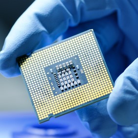 |
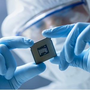
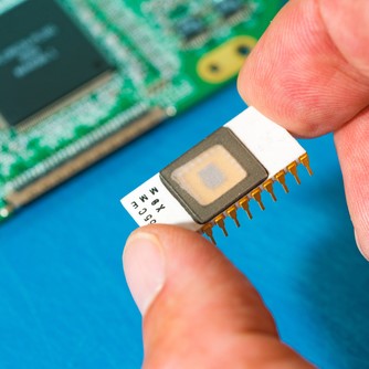
ChipA small section of a semiconductor wafer that contains a set of electronic circuits. Chips, short for “microchips,” act as the brains in our digital devices. |
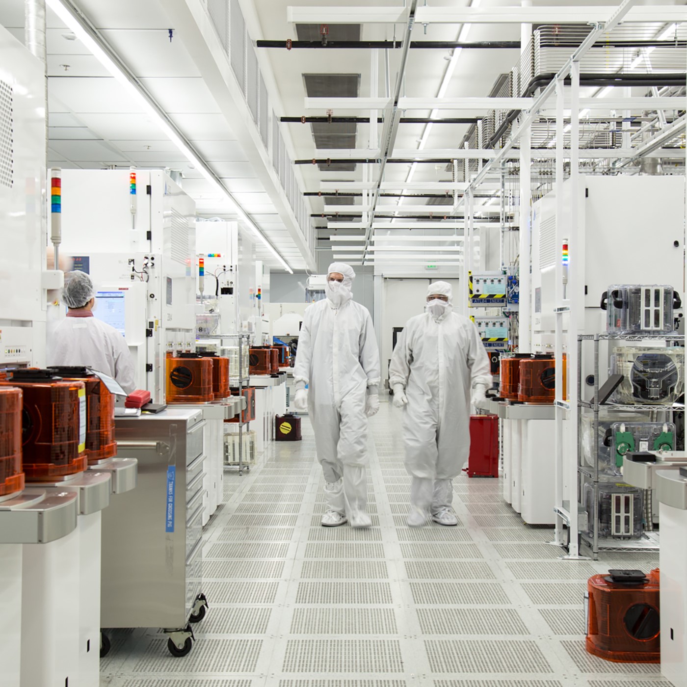 |
CleanroomThe ultra-clean room where chips are fabricated. The air in a cleanroom is thousands of times cleaner than the air in a hospital. |
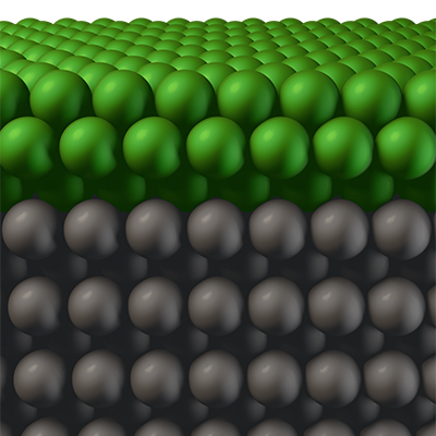 |
DepositionA process that lays down the materials on the surface of a wafer. Chemical vapor deposition (CVD), one of the most common methods of deposition, uses controlled reactions of volatile chemicals to deposit dielectric or conductive films on wafers. |
 |
EtchA process that selectively removes material to create desired patterns on a wafer. Material removal methods include dry (using plasma) and wet (using liquid chemistries) processes. |
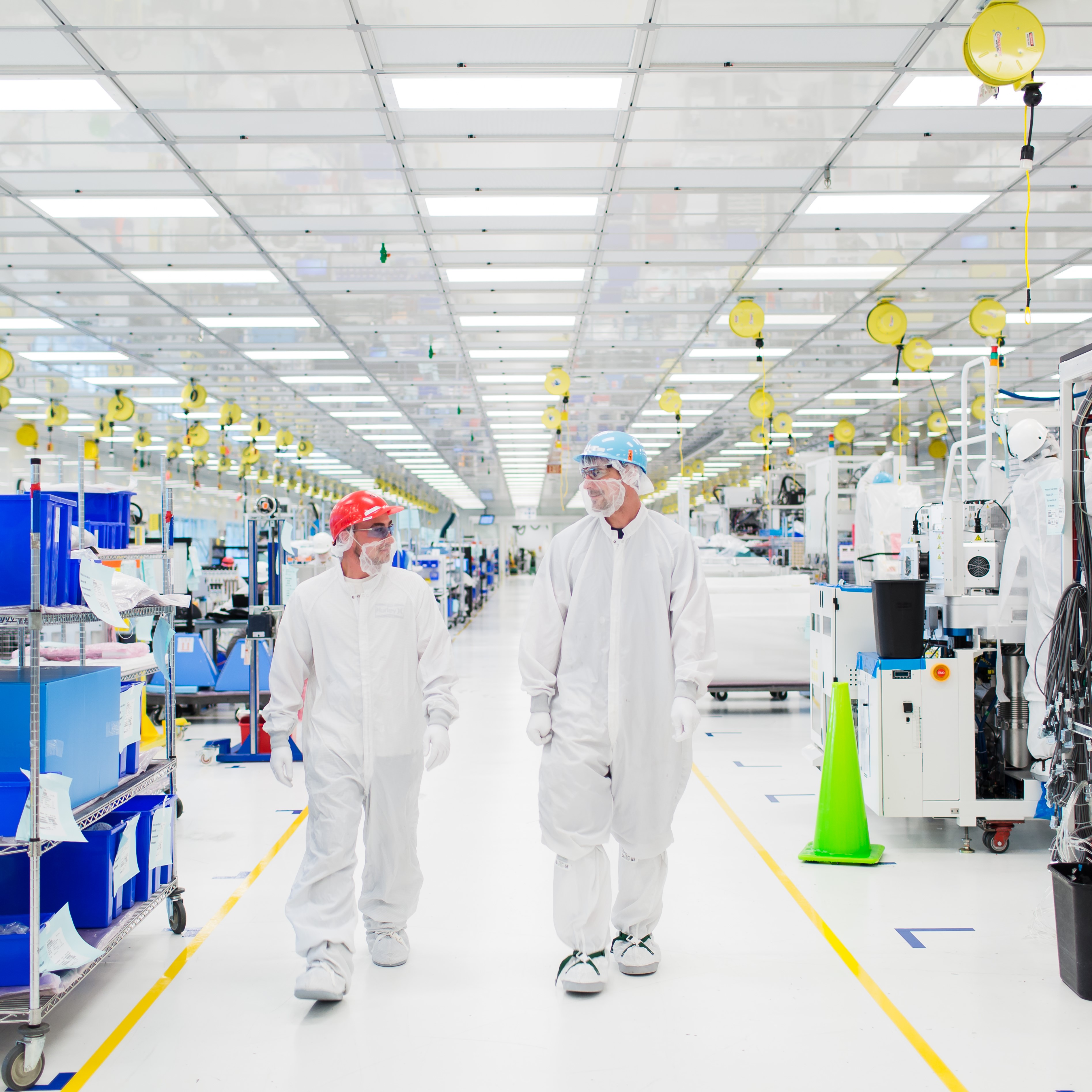 |
FabA manufacturing facility that creates semiconductor products. The cost of a new fab is estimated to be more than one billion dollars! |
 |
Integrated CircuitA network including components such as transistors and capacitors fabricated on the same substrate. There are three types of integrated circuits: digital, analog, and mixed. Digital integrated circuits use binary mathematics to turn on and off, analog integrated circuits filter and amplify continuous signals, and mixed integrated circuits contain both, analog and digital circuits, on a chip. |
 |
Moore’s LawAn observation made by Gordon Moore in 1965 and later revised in 1975 that the number of transistors on an integrated circuit would double every two years. His observation became the roadmap for research and development in the semiconductor industry. |
 |
PatterningThe process used to create patterns on a wafer that guide the deposition and etch processes. Patterning is the driving force behind scaling, allowing engineers to reduce the size of our transistors and their circuits. |
 |
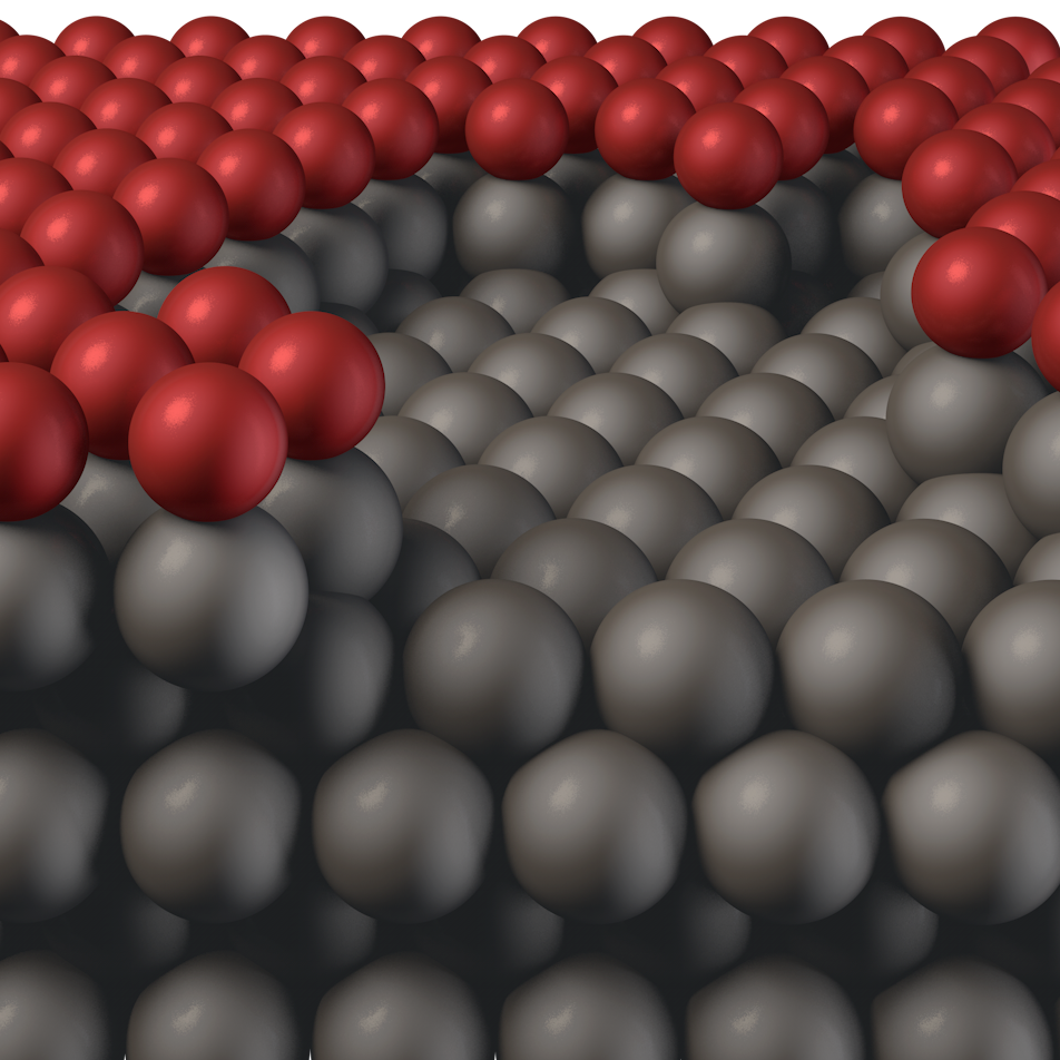
PlasmaA state of matter made up of free electrons and ions; created by sending a charge through a gas. Unlike typical gases, plasmas can conduct electricity because of their charged particles. |
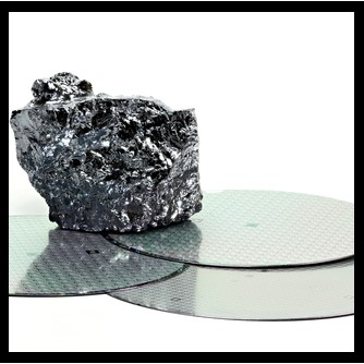 |
SemiconductorA material with electrical conductivity between that of a conductor and an insulator. Silicon is considered to be the world’s main semiconductor in chip making. |
 |
Technology NodeRefers to the device generation and its architectures; historically referred to gate length or half pitch. Today, technology node is now used as a nickname to refer to modified processes, rather than a physical feature on the device. |
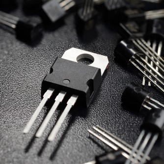 |
TransistorA type of device that is used to amplify or switch the flow of electricity. A chip can contain millions or billions of transistors! |
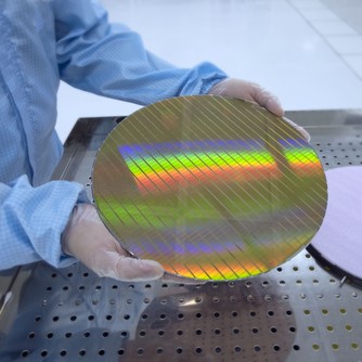 |
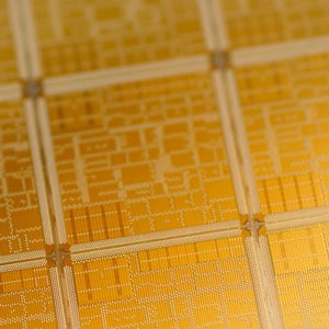
WaferA thin silicon disc made up of semiconducting material that is used to create chips. A 300 mm diameter wafer can hold 148 chips, assuming each chip is 20 mm x 20 mm. |
 |
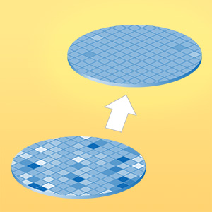
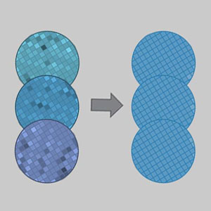
Wafer CleaningThe process of removing unwanted particles from the wafer during manufacturing. Without cleaning, impurities on a wafer can negatively affect the pattern, and hence, chip performance. |
Now that you’ve got the jargon down, you’re ready to join us in our labs! To check out more of our technical lingo, visit our website’s glossary.