Lam Executive Vice President and Chief Technology Officer, Richard A. Gottscho, gave a keynote at the SEMI Industry Strategy Symposium (ISS), the annual executive conference for the semiconductor industry. Titled, “I’m Living in a Little Data World, but I Have a Big Problem,” Rick talked about the challenges faced by the “little data world” of process development and the potential for new solutions on the horizon.
There are many examples today of what can be done with plentiful, cheap data. The availability of direct-to-consumer genetics testing kits have created big data pools from a large population. The combined and anonymized data can be tapped to develop medical solutions. As another instance, Rick talked about his wearable ring, which monitors his activity level, blood oxygen level, and sleep quality. Wearables generate lots of data for little cost. A key to advances in personalized medicine is the availability of large data sets that can be analyzed computationally.
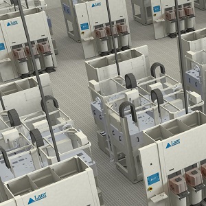
Shifting to our industry, a semiconductor fab generates extraordinary amounts of data: as a wafer goes through the fab, ~50 GB of data are generated by the wafer fabrication equipment and metrology and inspection tools. If chipmakers comingled and anonymized production data, every fab could have unprecedented productivity and yields, with both unit processes and integrated processes being optimized in close to real time.
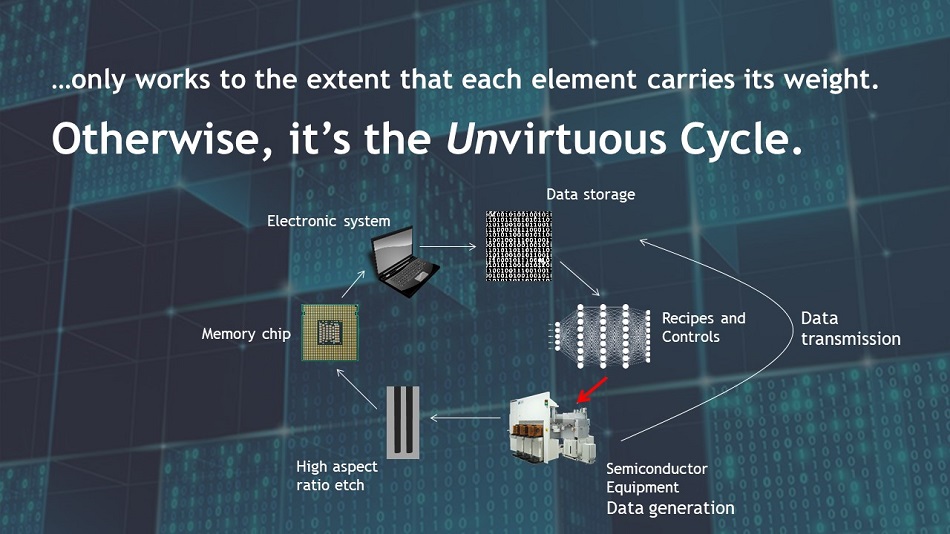
Today, “the pace of technological evolution has never been faster,” said Rick, and that extraordinary pace results from “a bunch of virtuous cycles of positive, exponential feedback.” As an example, he stepped through a semiconductor manufacturing cycle in which a recipe for high aspect ratio etch is fed into the etcher, eventually producing a chip that goes into an electronic system, which acquires data that can be processed and leads to a better recipe or better control of the process. With a number of such virtuous cycles in play, it is easy to understand the more than double exponential rate of technological evolution.

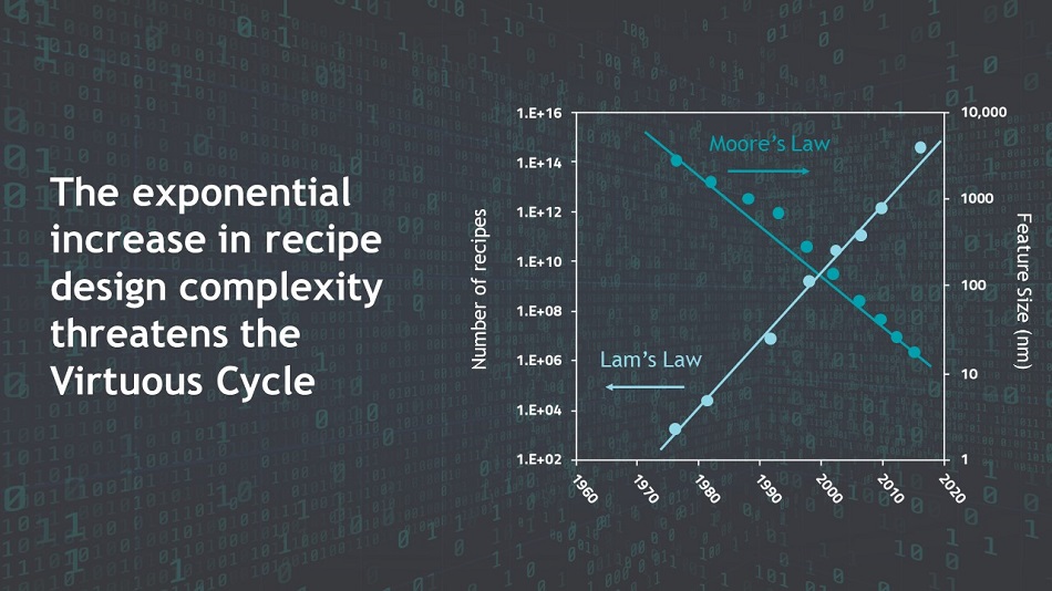
Process development, however, is getting more challenging as scaling progresses, and this threatens to slow the pace of technological evolution. As features on a chip have shrunk in size, the number of recipes has exploded exponentially – he shared this as a corollary to Moore’s Law, calling it Lam’s Law. To illustrate the point, Rick talked about high aspect ratio etching of a memory hole in a 3D NAND device and the incredible time and effort our world-class process engineers put in to perform the etch experiments as well as the (frequently, destructive) microscopy and other analytical work. However, there may be 1014 recipes to evaluate – an impractical number, from both a cost and time perspective. Unlike production, R&D has nearly an infinite number of choices and little data. A pure physics approach to the problem would also be impractical as there are too many unknowns and too little data.

Can a pure data-driven approach work? Simulations (in the form of a plasma etching “game”) have shown that the data-driven approach, even when guided by data scientists, lags what an experienced process engineer can accomplish in situations where we have limited data.
There are several reasons for optimism in the process development world, however. First, powerful computational capabilities exist today that allow us to model the plasma reactor complexity in three dimensions. Second, our seasoned process engineers can apply their domain expertise to simplify and reduce the problem to a handful of key parameters, which dramatically reduces the amount of data that needs to be generated to calibrate those parameters. Third, where orthogonalities exist (for example, the separation of surface modification from desorption in atomic layer etching), the dimensionality of the process optimization problem can be further reduced. And fourth, our ability to generate low-cost, useful data is growing rapidly.
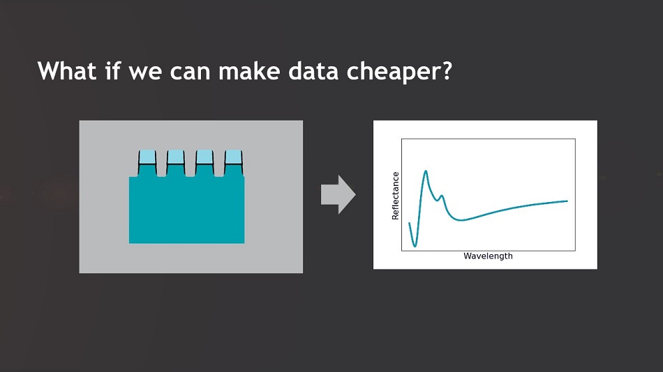
To demonstrate this last point, Rick shared Lam’s spectral reflectometry capability, which improves etch stop accuracy for trench etch, buried gate recess, and other applications where there is no etch stop layer. Process data is collected in situ, in real time, and non-destructively – all key to the cheap, abundant data goal, combined with the knowledge and expertise of our engineering teams, will help us maintain the remarkable pace of technological evolution that we have all come to enjoy and expect.

Rick is optimistic that while semiconductor equipment manufacturers may currently be living in a little data world, we will be able to capitalize on the benefits of big data in the not-too-distant future.