- BEOL module processing faces challenges as chipmakers move to the 3 nm node and beyond
- A semi-damascene integration scheme with airgap structures may help reduce RC delay time
As device scaling continues to the 3 nm node and beyond, back end of line (BEOL) module processing faces many new challenges. This is forcing chip makers to consider new BEOL integration schemes.
At the 3 nm node, state of the art Cu-metallization will be replaced by low resistance barrierless Ru-based BEOL metallization. The migration to ruthenium (Ru) for metallization is opening up the option for subtractive patterning. This approach, which combines subtractive patterning for minimum pitch interconnects along with conventional damascene for via structures, is also referred to as a semi-damascene integration.
An advantage of subtractive patterning for interconnect lines is that it provides an opportunity to migrate to high(er) aspect ratio (AR) metal lines. The drawback of this option, however, is that it can increase capacitance. This undesired effect can be overcome with the introduction of airgap structures to support interconnect line isolation. Hence, airgaps are envisioned as a main RC (resistance capacitance) delay time reduction booster.
The proposed semi-damascene integration scheme, combined with full-airgap integration, might be used at the most critical minimum pitch metal layers (M1 and M2). It can also be combined with conventional dual-damascene or hybrid metallization schemes.
Recently, we supported a study at imec to analyze advanced 3 nm node BEOL integration schemes. The integration of a semi-damascene flow with airgap structures was modeled using SEMulator3D® process simulation software. Using these simulations, imec achieved a better understanding of the integration challenges and associated failure risks prior to proceeding with silicon wafer processing in the pilot line. The goal of this project was to help imec define process assumptions for 3 nm BEOL integration using semi-damascene integration and airgap structures.
Flow Simulation
The semi-damascene airgap process flow for a 3 nm BEOL scheme was simulated using SEMulator3D. Figure 1 illustrates the key process steps, which included an M1 Ru etch step, airgap closure after an M1 Ru etch, FSAV (fully self-aligned via) patterning, FSAV/M2 metallization, and finally M2 patterning.
For this simulation, the M1 Ru patterning and airgap closure process steps were calibrated based on imec TEM images for a 10 nm half-pitch metal interconnect module, to realistically reproduce the airgap shape.
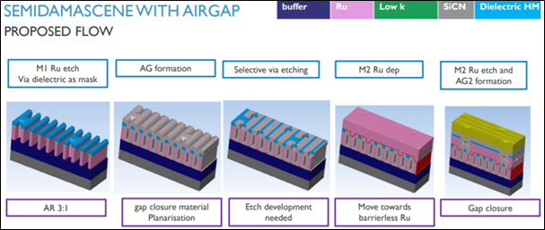
Figure 1: Semi-damascene airgap process flow for 3 nm node BEOL.
Airgap Challenges
Using SEMulator3D, the challenges and the weak points related to airgap closure during a semi-damascene airgap process flow were investigated to avoid potential Si-wafer processing failures.
Figure 2 illustrates the challenges of the 3 nm node semi-damascene airgap process. Figure 2 highlights that planarization after airgap closure is required to maintain dielectric constant (k) value and conformality. Furthermore, airgap closure control was distinguished as a key process challenge.
Our simulation demonstrated that there is a minimum distance between M1 and M2 that should be preserved to avoid an airgap open failure. More specifically, it was found that in the first step of the FSAV (fully self-aligned via) etch, processes must be used that have high selectivity to the exposed SiCN airgap closure dielectric material.
For the subsequent silicon copper nitride (SiCN) etch process steps, an etch process that provides a high taper of the SiCN dielectric is required to connect to the underlying Metal 1 Ru. This decreases over etching of the gap closure dielectric and helps maintain the airgap closure during the via etch process. The necessary SiO2 to SiCN etch selectivity, and the desired SiCN taper, are respectively illustrated by our simulation results in the left and right images shown in Figure 3.
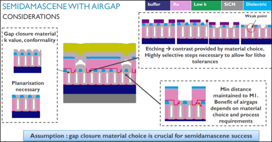
Figure 2: Semi-damascene airgap process flow challenges.
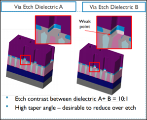
Figure 3: Airgap closure weak point challenge.
Sensitivity Analysis
During simulation, we performed a sensitivity analysis of the process parameters that could control and maintain the airgap closure and volume. A total of 200 Monte Carlo runs using SEMulator3D were launched, varying the M1 litho CD, thickness of the SiCN gap-closing dielectric, SiO2 hard mask thickness, M1 Ru lateral etch and Ru-height. Details regarding the process parameters and the associated parameter ranges assessed are reported in Figure 4.
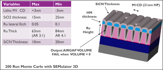
Figure 4: Airgap closure process sensitivity analysis.
The simulation demonstrated that the biggest contributors to airgap closure failure were the Metal 1 CD, where a smaller CD increased the risk for failures during the SiCN deposition, and a smaller SIO2 hard mask thickness. Additionally, Metal 1 Ru thickness and SiO2 HM thickness were identified as the biggest contributors to airgap volume (Figure 5).
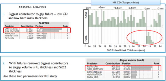
Figure 5: Results from process sensitivity study: impact study for airgap closure failure (top) and impact study related to airgap volume.
The results of the airgap volume sensitivity studies were used to quantify the impact on RC reduction. The results from this analysis are reported in Figure 6.
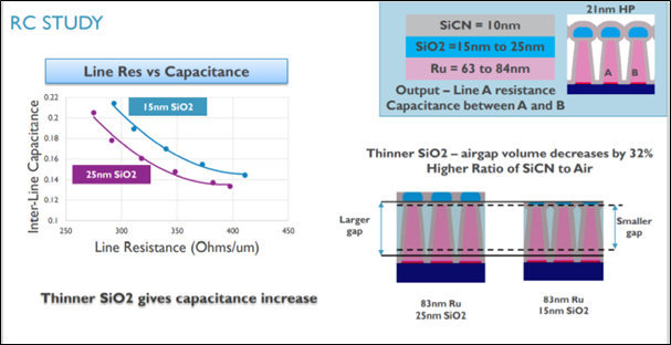
Figure 6: Airgap volume process sensitivity study and corresponding impact on RC reduction.
Key Takeaways
In this study, a semi-damascene airgap process flow for BEOL at the 3 nm node was simulated using SEMulator3D. Weak points and process challenges were investigated to define optimal processes for a 3 nm node BEOL scheme using the proposed semi-damascene flow.
Process flow simulations indicated that airgap material choice and etching processes were crucial to successful yield of the semi-damascene and airgap process scheme. These process models were invaluable, since imec could study key processes of a proposed 3 nm BEOL process scheme without resorting to time-consuming and expensive silicon wafer fabrication.
Dr. Assawer Soussou is a semiconductor process and integration (SPI) engineer within Semiverse™ Solutions at Lam Research. She has 10+ years of experience in semiconductor process engineering, including positions at ST Microelectronics and CEA-Leti from 2010-2105 where she worked in device modeling, characterization and reliability engineering of BEOL, MOL, metal, high K and SiGe architectures. She subsequently worked at Altis Semiconductor and XFAB in new technology development, qualification and electrical characterization for CMOS and other device architectures. Dr. Soussou joined Lam in March 2018, and is currently working for the Semiverse Solutions group in Europe, where she is responsible for advanced nanotechnology development and process modeling projects with Lam’s key partners and customers. She received her Ph.D. in Microelectronics & Electronics from the Institut Polytechnique de Grenoble, in Grenoble, France.
Acknowledgment
The author gratefully acknowledges Gayle Murdoch and imec for allowing us to share this work. This research was supported by the Pin3s ECSEL Joint Undertaking.