Reducing the parasitic capacitance between the gate metal and the source/drain contact of a transistor can decrease device switching delays. One way to reduce parasitic capacitance is to reduce the effective dielectric constant of the material layers between the gate and source/drain. This can be done by creating airgaps in the dielectric material at that location. This type of work has been done in the past for back-end-of-line (BEOL) to reduce the capacitance between interconnects [1-4]. In this work, we focus on the front-end-of-line (FEOL) and demonstrate a SEMulator3D® model of an airgap created between the gate and source/drain [5]. SEMulator3D® is a virtual fabrication software platform that can model process variability within a given semiconductor process flow. Using the Design of Experiment (DoE) capabilities in the SEMulator3D® tool, we show the dependence of the parasitic capacitance on the etch depth and other etch process parameters used to create the airgap. Additionally, we show the dependence on the size and volume of the airgap.
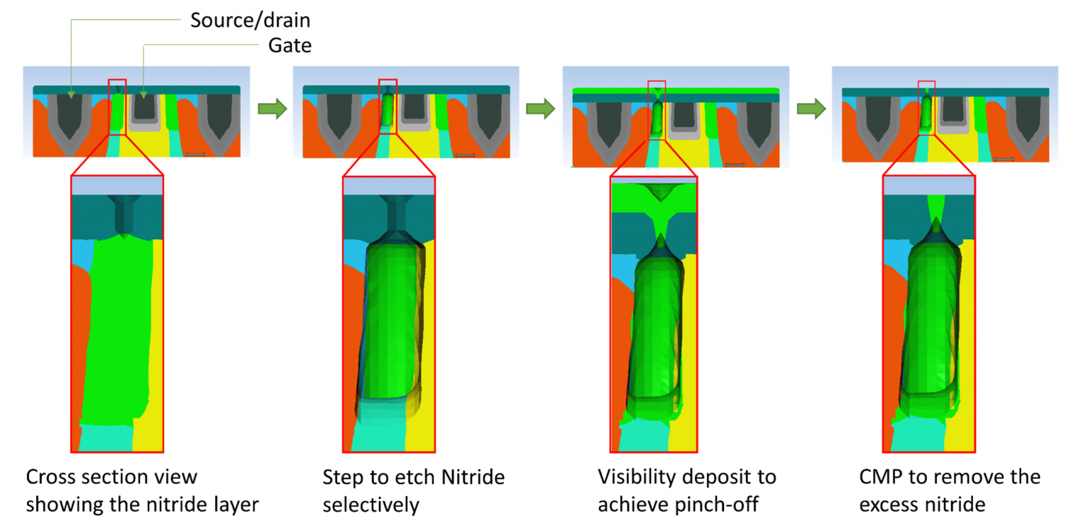
Figure 1 displays a cross-section view of a SEMulator3D® FinFET model. To create an airgap between the gate and the source/drain of the FinFET, a highly selective silicon nitride etch process is implemented, followed by a silicon nitride deposition process which is optimized to pinch off and create the airgap. A silicon nitride CMP process is then used to planarize the surface.

Figure 1 – SEMulator3D® process flow for creating an airgap in a FinFET model. The visibility deposit step creates the airgap by pinching off the airgap at the top. The CMP step is then used to remove the excess nitride. Scale bar is 10nm. The airgap reduces the parasitic capacitance between gate and source/drain. The size of the airgap can be controlled by varying the etch depth, tilt and source sigma of the etching reagents.
Using SEMulator3D’s virtual metrology capabilities, the following metrics were then measured:
- Parasitic capacitance between the gate metal and S/D contact
- Volume of the airgap
- Z-axis minimum of the airgap which is representative of the vertical size of the airgap
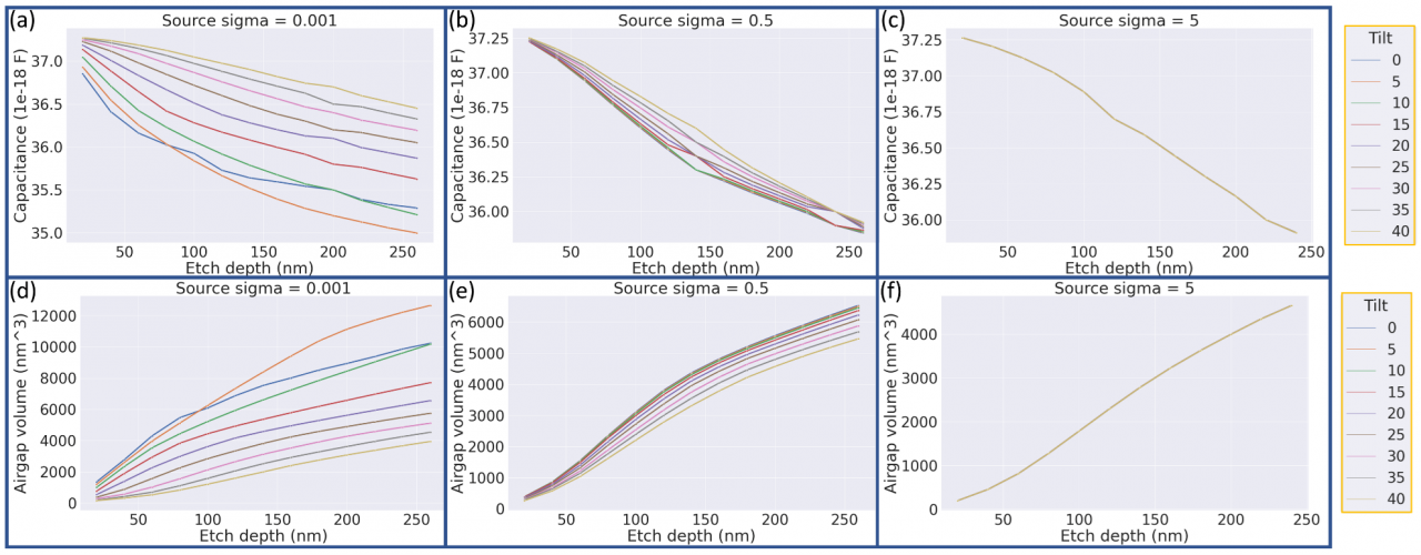
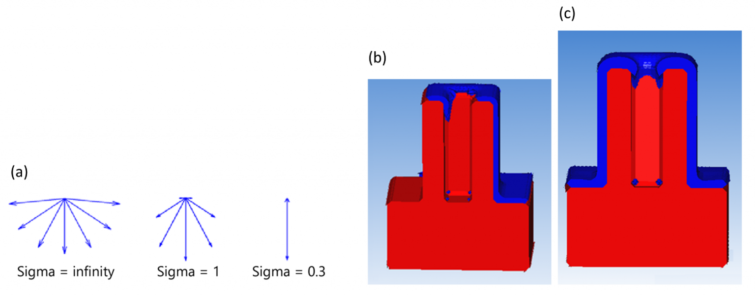
During the silicon nitride etch step, the etch depth, the angular spread of the etching reagents (referred to as source sigma in the literature) and the tilt angle (with the wafer assumed to be rotating) were varied during the DoE. Figure 2(a-f) show how the capacitance and volume of the airgap varied with the etch depth for different values of tilt and source sigma. As the etch depth is increased, we create a larger airgap (Figure 2 d). This decreases the effective dielectric constant since air’s dielectric constant is much lower than that of the nitride. This in turn, reduces the parasitic capacitance between the gate and source/drain. A decrease in the tilt angle has the effect of moving the etching reagents away from the side walls and towards the bottom of the resulting airgap (Figure 3 b-c). This explains the larger airgap (and lower capacitance) for a given depth and source sigma, as we decrease the tilt (Figure 2 a & d). Another significant result is that as the source sigma increases, the effect of tilt decreases. When the source sigma is set at 5, corresponding to a broad/isotropic angular spread, tilt has no effect at all on the capacitance and airgap volume (Figure 2 c & f). This is consistent with the how increasing source sigma affects etching. Increasing the source sigma makes the etching reagents hit the substrate in a more isotropic manner (Figure 3 a). This means that the tilt no longer impacts the etching behavior as it does at lower source sigma values.

Figure 2 – As the etch depth is increased, airgap volume increases and the parasitic capacitance decreases (Figure 2 a & d). This decrease is steeper when the tilt angle is lower. However, the effect of tilt decreases as the source sigma is increased. When source sigma is 5, tilt has no effect on the capacitance and airgap volume (Figure 2 c & f).

Figure 3 – (a) Effect of Angular Spread (Sigma) on the directionality of the etching reagents (b) Effect of a tilt of 45 degrees shown (wafer fixed) (c) Effect of a tilt of 80 degrees (wafer rotating). Image source: SEMulator3D product documentation
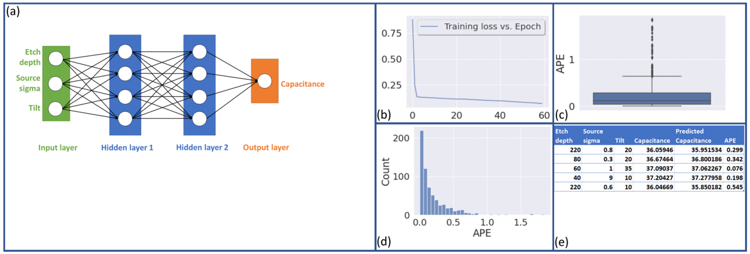
Running a large DoE is a time and computational resource intensive process. While it is necessary to do this for process optimization, any reduction in the parameter space of the DoE helps reduce the time and resources needed. A machine learning model that can predict outcomes based on independent variables is useful as it reduces the need for running the DoE for all combinations of the independent variables. With this goal in mind, the data collected in this DoE was fed into an artificial neural network (ANN) after splitting the data into training (70%) and testing (30%) sets. The model had two hidden layers (Figure 4 a). The grid search method was used for hyper parameter tuning. The model was run on the test data and found to have a mean accuracy of 99.8%. Three quarter of test cases had an absolute percent error (APE) of 0.278% or lower (Figure 4 c). Figure 4 e displays a sample of test rows with the predicted and actual parasitic capacitance. This application of machine learning (ML) allows us to reduce the size and time needed for the DoE. We can reduce the parameter space substantially without reducing the accuracy of the results significantly. In our case, the DoE size was reduced from ~5000 to ~2000 parameter combinations. SEMulator3D’s custom python step integrates this type of machine learning code into the process simulation, and the results can be fed to the next step in the semiconductor process model.

Figure 4: An Artificial Neural Network (ANN) model is used to predict the parasitic capacitance of an airgap between the gate and source/drain of a FinFET device. Figure 4(a): A neural network is built using the etch depth, tilt and source sigma as inputs to the model. The neural network has an input layer, 2 hidden layers, and an output layer. Figure 4(b): A graph of training loss (%) vs. Epochs (number of training cycles). Figure 4(c): Distribution graph of Absolute Percentage Error (APE), which is the metric used to measure the difference between the predicted capacitance and the actual capacitance. The prediction accuracy on the test data was found to be 99.8%. Figure 4(d): A graph of trial count (incidence) vs. Absolute Percentage Error. 75% percent of test cases had an APE of 0.28% or lower. Figure 4(e): A table containing a sample of test rows and data with the predicted and actual parasitic capacitance. Etch depth, source sigma, tilt, capacitance, predicted capacitance and APE values are all shown in the table. An accurate machine learning model allows a smaller parameter space to be explored and hence lower time and computational resources.
Conclusions
Coventor SEMulator3D® was used to create a virtual airgap between the gate and the source/drain of a FinFET device. The impact of this airgap on parasitic capacitance was studied. Etch process parameters were varied and the impact on the airgap volume and parasitic capacitance was also studied. The results were fed into an artificial neural network to create a machine learning model that can predict parasitic capacitance, thereby reducing the need to run a DoE for every combination of etch parameter values.
References
[1] Hargrove, M. (2017, October 18). Reducing BEOL Parasitic Capacitance using Air Gaps https://www.coventor.com/blog/reducing-beol-parasitic-capacitance-using-air-gaps
[2] Nitta, S., Edelstein, D., Ponoth, S., Clevenger, L., Liu, X., & Standaert, T. (2008, June). Performance and reliability of airgaps for advanced BEOL interconnects. In 2008 International Interconnect Technology Conference (pp. 191-192). IEEE.
[3] Shieh, B., Saraswat, K. C., McVittie, J. P., List, S., Nag, S., Islamraja, M., & Havemann, R. H. (1998). Air-gap formation during IMD deposition to lower interconnect capacitance. IEEE Electron Device Letters, 19(1), 16-18.
[4] Fischer, K., Agostinelli, M., Allen, C., Bahr, D., Bost, M., Charvat, P., … & Natarajan, S. (2015, May). Low-k interconnect stack with multi-layer air gap and tri-metal-insulator-metal capacitors for 14nm high volume manufacturing. In 2015 IEEE International Interconnect Technology Conference and 2015 IEEE Materials for Advanced Metallization Conference (IITC/MAM) (pp. 5-8). IEEE.
[5] Banna, S. (2016, August). Scaling challenges and solutions beyond 10nm. In 2016 IEEE International Conference on Electron Devices and Solid-State Circuits (EDSSC) (pp. 181-186). IEEE.