Month Year
| Su | Mo | Tu | We | Th | Fr | Sa |
|---|---|---|---|---|---|---|
Month Year
| Su | Mo | Tu | We | Th | Fr | Sa |
|---|---|---|---|---|---|---|


 |Jun 14, 2023|
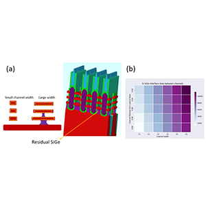
As transistor sizes shrink, short channel effects make it more difficult for transistor gates to turn a transistor ON and OFF [1]. One method to overcome this problem is to move away from planar...
 |Jan 13, 2023|
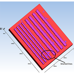
Line edge roughness (LER) can occur during the exposure step in lithography [1-2]. Similarly, etch and deposition process steps can leave a roughness on semiconductor surfaces. LER is a stochastic...
 |Oct 27, 2022|
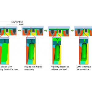
Reducing the parasitic capacitance between the gate metal and the source/drain contact of a transistor can decrease device switching delays. One way to reduce parasitic capacitance is to reduce...