As transistor sizes shrink, short channel effects make it more difficult for transistor gates to turn a transistor ON and OFF [1]. One method to overcome this problem is to move away from planar transistor architectures toward 3D devices. Gate-all-around (GAA) architectures are an example of this type of 3D device [2]. In a GAA transistor, the gate oxide surrounds the channel in all directions. A key process during the fabrication of GAA transistors involves the channel release step. This process step is used to etch away the SiGe that has been deposited between the Si nanosheets [3]. An ideal etch process would remove all of the SiGe without removing any silicon. In practice, however, process engineers perform a trade-off between leaving some residual SiGe and over etching the surrounding silicon. An aggressive etch process that removes all residual SiGe can lead to undesirable silicon loss. On the other hand, attempting to minimize the silicon loss can cause residual SiGe to remain after the channel release step, leading to suboptimal device performance.
These tradeoffs between residual SiGe, silicon over etching and channel width can be better understood using semiconductor process simulation and virtual process window exploration. Using this technique, a virtual design of experiment that varies the etch time, etch lateral ratio, etch selectivity (between SiGe and Si) and channel width can be completed, to determine an optimal set of tradeoffs during the GAA channel release process. The residual SiGe is characterized by measuring (virtually) the contact area between the silicon and SiGe within the nanosheets (while ignoring the epitaxially grown Source/Drain SiGe).
The virtual design of experiments described in this article was completed using the Expeditor module of SEMulator3D® [4] running on a high-performance computing (HPC) infrastructure. The channel width was varied using the y-bias of the lithography step used to create the active area of the device. The etch lateral ratio, etch selectivity, and etch time were also varied as DOE parameters.

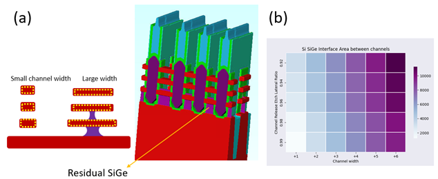
Figure 1: A virtual model of a GAA FET showing residual SiGe after the channel release step. Process engineers have to make a trade-off between silicon loss and residual SiGe.(b) Variation in residual SiGe as a function of the channel width and etch lateral ratio. The higher the channel width, the higher the lateral ratio needed to etch away all the SiGe. Channel widths are shown as delta values from the nominal value of 30 nm.
As shown in Figure 1, SiGe can be found between the Si nanosheets and requires an SiGe etch in the lateral direction. A large channel width can interfere with this lateral etch process. Avoiding residual SiGe puts an upper limit on the channel width, which in turn limits the current carrying capacity of the device.
In our virtual experiments, we increased the channel width from its nominal value of 30 nm to determine the impact of a larger channel width. Figure 1b shows the variation of the residual SiGe as a function of channel width and lateral etch ratio. As expected, a larger channel width requires a higher lateral etch ratio to completely etch away the SiGe. If the lateral ratio isn’t high enough, some SiGe remains between the Si nanosheets.

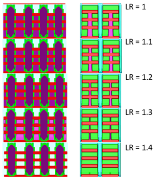
Figure 2: A cross section view of a GAA FET virtual model. This figure displays the effect on residual SiGe as the lateral ratio is varied from 1 to 1.4 while the channel width is increased from a nominal value of 30 nm to a value of 42 nm. As can be seen in the side views on the right compared to the case in Figure 1, much higher lateral ratios are required to completely etch all of the SiGe between the nanosheets.
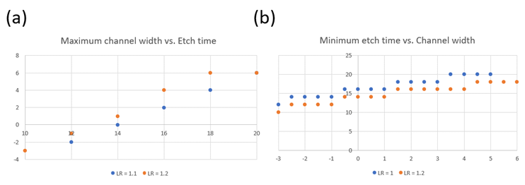
Figure 2 shows the results of varying the etch lateral ratio on the amount of residual SiGe using a device that has a larger channel width (nominal + 6 nm). As the channel width increases, the lateral ratio needed to fully etch all of the SiGe increases. In Figure 3, we highlight the relationship between channel width and etch time that is needed to etch away all of the SiGe. As we increase the etch time, the maximum channel width can be increased without leaving any residual SiGe (Figure 3a). As the channel width increases, the minimum etch time required to etch all of the SiGe also increases, as expected (Figure 3b).

Figure 3: (a) As we increase the etch time, the maximum channel width that can be supported without any residual SiGe increases. (b) As the channel width increases, the minimum etch time to etch all of the SiGe also increases. Channel widths are shown as delta from the nominal value of 30 nm.
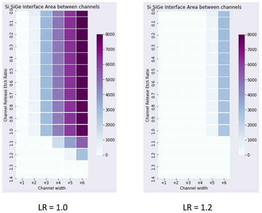
In the results so far, we have assumed that there is an infinite etch selectivity between Si and SiGe. As a next step, we brought etch selectivity into our experiment. We varied the etch selectivity between Si and SiGe, and looked at the impact of these changes on the channel release process (Figure 4). To support a higher channel width, we found that we needed to increase either the etch selectivity or the lateral ratio of the etch process.

Figure 4: Variation of Residual SiGe with etch selectivity and channel width for two different etch lateral ratios. A higher lateral ratio etches more SiGe and allows higher channel width for any given etch selectivity. Channel widths are shown as delta from the nominal value of 30 nm.
From these plots, we can derive the process windows necessary to achieve targeted device characteristics (and performance) for our GAA device. For instance, with a lateral ratio of 1, and an etch time of 20 seconds, the channel width will need to be in the 37 to 40 nm range, to achieve zero residual SiGe and optimal device performance.
Conclusions
A virtual design of experiment was performed to study the relationship between residual SiGe, etch ratio, etch selectivity, and channel width during the GAA transistor channel release process. This type of virtual process window exploration can be used to quickly optimize process parameters during the development of advanced GAA transistor architectures, without the need for costly and time-consuming wafer-based experimentation.
References
[1] Xie, Q., Xu, J., & Taur, Y. (2012). Review and critique of analytic models of MOSFET short-channel effects in subthreshold. IEEE transactions on electron devices, 59(6), 1569-1579.
[2] Mukesh, S., & Zhang, J. (2022). A Review of the Gate-All-Around Nanosheet FET Process Opportunities. Electronics, 11(21), 3589.
[3] Sun, X., Wang, D., Qian, L., Liu, T., Yang, J., Chen, K., … & Zhang, D. W. (2023). A Novel Si Nanosheet Channel Release Process for the Fabrication of Gate-All-Around Transistors and Its Mechanism Investigation. Nanomaterials, 13(3), 504.
[4] SEMulator3D® Coventor, Inc. https://www.lamresearch.com/products/semulator3d/