- Lam Research was the platinum sponsor of the 27th gathering of SEMICON Taiwan, held September 14 to 16.
- More than 45,000 attendees examined 2,450 exhibition booths showing the latest industry trends and technological progress.
Lam’s experts were invited to SEMICON Taiwan to give keynote speeches at the MEMS & Sensor Forum, Smart Manufacturing Forum, IC Forum, and Heterogeneous Integration Global Summit. Lam was also invited to speak at the “Workforce Development Program – Women in Semiconductor (WiS) Seminar” to discuss women’s leadership in the STEM field.
Here is a recap of the main presentations from Lam Research participants at SEMICON Taiwan 2022.
Click here to see job openings at Lam
MEMS & Sensors Forum
In his speech “Addressing High Volume Manufacturing Challenges and Technology Inflections in MEMS,” Dr. David Haynes, vice president of strategic marketing, Customer Support Business Group at Lam Research, said MEMS sensing devices are rapidly evolving into the new field of smart sensors.
- MEMS is expected to gain wider application in the automotive, Internet of Things, 5G, smart home, and other markets.
- Moreover, MEMS and MEMS fabrication technologies are expected to play a key role in enabling the metaverse.
Lam Research has formulated three strategies to help customers overcome MEMS’s high-volume manufacturing challenges:
- Leverage Lam’s leading-edge technology to enable MEMS process capability
- Address MEMS and sensor customers’ high value challenges
- Be a partner in MEMS and sensor development and process optimization
Haynes points out that Lam Research has launched the Syndion® family of products for 300mm wafers and is developing a new generation of DSiE technology specifically for the needs of the MEMS market.
- In addition, Lam is actively investing in the development of new materials, lifetime extension of production tooling, and 200-300mm extendibility.
The industry is also developing a new generation of piezoelectric MEMS devices to drive the paradigm shift for MEMS devices. Since piezoelectric materials are non-volatile materials used in the etching process, they are more difficult to fabricate.
Smart Manufacturing Forum
Dr. Joseph Ervin, senior director of the Semiconductor Software Products Group at Lam Research, discussed the challenges and solutions at 3nm and beyond in a presentation entitled “Using Digital Twins, Predictive Process Models and Advanced Material Engineering in Next Node Semiconductor Development.”
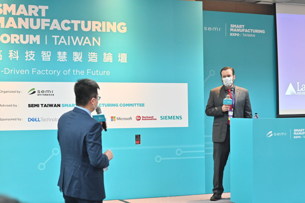
Joseph Ervin takes a question from the audience
Ervin explains that by using 193nm immersion lithography (193i) with multiple patterning, chipmakers have been able to generate advanced features down to 7nm. Using 193i lithography has become increasingly problematic at 5nm and beyond, due to the large number of patterning and process steps required at smaller feature sizes.
- With the advent of Extreme Ultraviolet (EUV) lithography, the most difficult features at 3nm and beyond can now be patterned.
- As a result, EUV has become the industry choice for patterning the latest nodes, due to its improved dimensional resolution and simplification of patterning and processing.
Unfortunately, transitioning to EUV lithographic exposure is likely insufficient on its own. 193i was a long-life lithography technology, and lithography scaling alone at 193i was not sufficient to scale logic at earlier semiconductor nodes.
- Different integration technologies are needed for 193i lithography, such as self-aligned double-patterning (SADP) and self-aligned quadruple patterning (SAQP), cut-block, material innovation, design technology co-optimization (DTCO), self-aligned patterning, and others.
- Patterning specifications are extraordinarily challenging at 3nm, with processes that approach the boundaries of physics. Yield can be impacted by unwanted variations and stochastic-induced defects during EUV processing, creating unintentional line edge roughness (LER), line width roughness (LWR), and edge placement error (EPE).
- Compounding these issues, lithography, patterning, and downstream processes must be co-optimized to have an acceptable yield and cost outcome.
Predictive process models, digital twins, automated variability control, and material optimization technologies can be used to develop next-generation devices using EUV lithography.
- Material innovations, holistic patterning, integration, manufacturing control, and DTCO will continue to be needed at 3nm and below, even with EUV lithography.
- By combining EUV dry photoresist techniques, advanced process models, holistic patterning, and co-optimized integration, Ervin says EUV lithography should be able to scale to 3nm and beyond.
Click here to see job openings at Lam
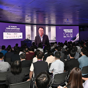
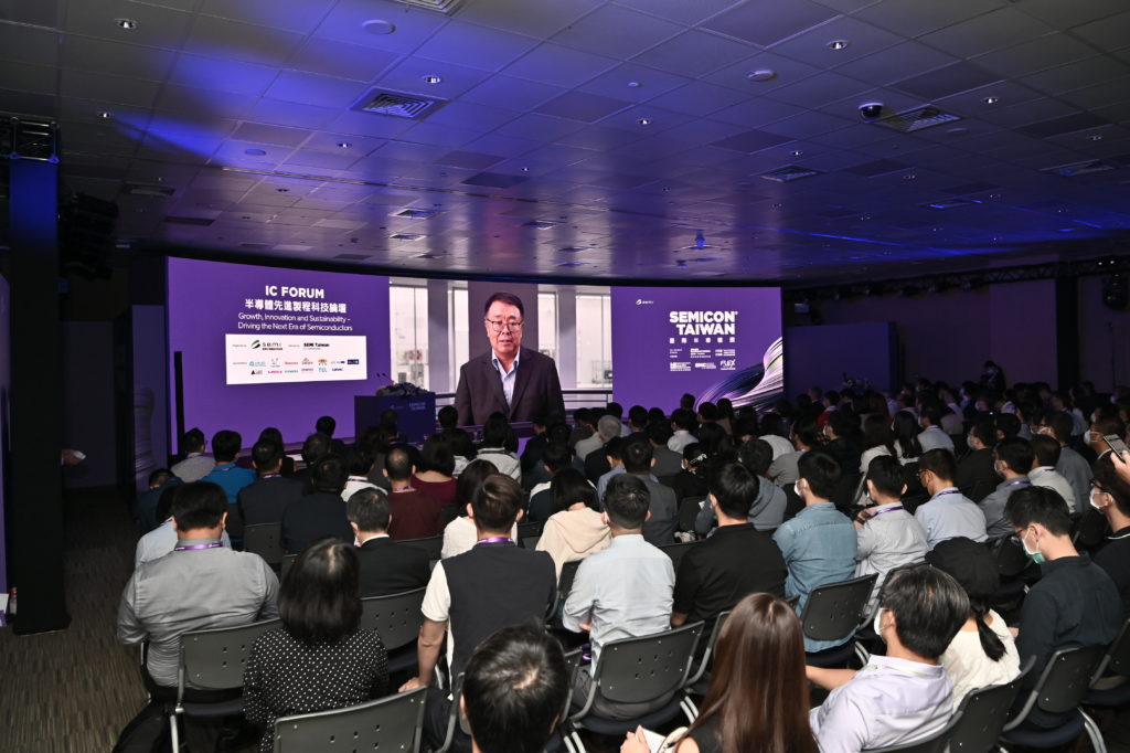
IC Forum
Dr. Yang Pan, corporate vice president of Advanced Technology Development at Lam Research, introduced “Dry Photoresist System for EUV Patterning,” saying that Lam’s dry photoresist deposition and dry development technology is a breakthrough approach for next-generation logic and DRAM devices that is expected to help enable everything from machine learning and artificial intelligence to mobile devices.
Yang Pan presented virtually
- EUV dry resist excels in terms of EUV absorption, basic unit size, stochastics, and pattern collapse.
- EUV dry resist system enables excellent performance and cost through co-optimization of unit process.
- “This innovative technology breaks the tradeoffs between dose, roughness, and defect performance,” says Pan.
To achieve extremely low EUV patterning defects at low dose, Lam Research has engineered a holistic approach to co-optimize the complete EUV patterning flow with key differentiating steps, such as dry photoresist deposition, post-exposure bake (PEB), dry development, and pattern transfer etch.
- Dry photoresist can provide a simple, homogeneous, and stable composition of metal oxide network after deposition, EUV exposure, and PEB.
- The materials contrast of dry photoresist is enhanced by proprietary underlayer technology and PEB optimization to obtain enhanced selectivity for dry development and downstream pattern transfer etch.
- Dry development allows Lam to tune the conditions during the pattern development process to provide optimum dry photoresist integrity and mitigate any residue for patterned defect performance.
- Dry development offers key sustainability benefits by consuming less energy and five to ten times fewer raw materials than traditional resist processes.
Pan further explains that Lam’s dry EUV patterning system can be extended to define pillars and holes at pitches for future logic and memory technologies using high numerical aperture extreme ultraviolet lithography (NA EUV) technology.
Integration Global Summit
In recent years, heterogeneous integration has driven packaging innovation for high-end applications like application processors (AP) and high-performance computing (HPC). These applications drive smaller features in the fan-out wafer level packaging (FO-WLP) and substrate markets. To provide better cost-effectiveness and expand the application scope of fan-out technology, fan-out panel level packaging (FO-PLP) has become another option for chipmakers.
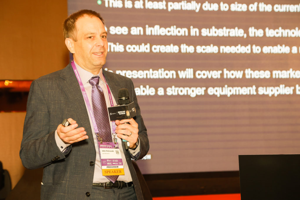
John Ostrowski talked about fan-out technology
- However, there are still many difficulties to be overcome on the panel level process.
- John Ostrowski, managing director of SABRE 3D at Lam Research, addressed these issues in his speech, “Equipment Challenges for Panel Level Processing.”
Ostrowski says that since the low-cost fan-out process technology on panels is not mature, yields are low, which limits the FO-PLP market size. The industry has not yet invested heavily in the research and development of FO-PLP.
- With a small market and no clear path to increase volume few companies have been willing to invest significant R&D money to solve these yield issues.
Ostrowski says the technical requirements for FO-PLP and substrates are converging and that the volume and growth in the substrate market is significant. The convergence of both panel markets is expected to create the volumes needed to allow more R&D investments into the panel market to help solve the key issues limiting yields.
- As a result, investments should increase as volume increases and improving panel yield should drive more panel volume in a positive feedback loop.
Another issue with panel-level packaging has been the lack of standards. Traditionally many different sizes of panels have been used in the industry. That issue appears to be resolving itself. For substrates, 510mmx515mm and for FO-PLP 600mmx600mm panels are becoming the standard.
- Beyond panel size, the interface and equipment standards are also important to allow for a common equipment set to be used for both applications.
Ostrowski notes that the convergence of the technical requirements on substrates and FO-PLP will lead to the adoption of more standards. Our efforts will be around developing a common system platform to reduce costs and address challenges, including defect control, uniformity control, productivity, and cost-effectiveness.
Workforce Development Program – Women in Semiconductor (WiS) Seminar
This year’s Women in Semiconductor (WiS) Seminar was titled “Unleash the Potential of Woman Leadership.” Annie Chou, director of Spares Operation & Logistics at Lam Research, and other outstanding female executives were invited to discuss and share their experiences working in the semiconductor industry.

Annie Chou encouraged women to seize opportunities
- Chou, who previously worked in Lam’s finance department, stepped out of her comfort zone when she joined a job rotation program to support internal and external customers on the front line.
- She encourages women in the industry to be brave to seize opportunities and build a better career.
Read an interview with Soon Kuek, the head of operations in Lam Malaysia and Alyson Crafton, head of the Global Information Systems’ (GIS) Common Services Organization
As the semiconductor industry continues to progress along “More Moore” to 3nm and beyond, as well as to create “More than Moore” opportunities for heterogeneous integration and special processes, Lam Research demonstrated its technological strength at SEMICON Taiwan 2022.
Lam continues to invest in advanced process development, EUV dry photoresist, high volume manufacturing of MEMS, and heterogeneous integration in response to industry trends. Lam Research will resolutely pursue innovation, push the boundaries of technological limitations, and develop solutions that keep semiconductor manufacturing moving forward.
Click here to see job openings at Lam
Frances Huang works in Communications and is based in Taiwan
This article contains forward-looking statements within the meaning of the Private Securities Litigation Reform Act of 1995. Forward-looking statements include any statements that are not statements of historical fact, including statements regarding: anticipated business results; market, industry and industry segment expectations; product development and release plans; product performance; customer and industry demand; and our ability to successfully execute business, product and growth plans or strategies. Forward-looking statements are subject to risks and uncertainties that could cause actual results to differ materially from the expectations expressed, including the risks and uncertainties described in our filings with the U.S. Securities and Exchange Commission, including specifically the Risk Factors described in our annual report on Form 10-K and quarterly reports on Form 10-Q. You should not place undue reliance on forward-looking statements. We undertake no obligation to update any forward-looking statements.