
The IoT and automotive markets use devices fabricated at a wide range of technology nodes. Taking advances made at 300 mm and applying them via upgrades to 200 mm equipment is a cost appropriate strategy to quickly improve yield and add capacity.
The industry is no longer held captive by sales from computing applications, such as personal computers, servers or even cellular phones and tablets. A diverse range of markets are contributing to growth seen by Lam and our customers. Cloud storage, machine learning or artificial intelligence (AI), virtual reality (VR) and augmented reality (AR), robotics, medical and automotive, including the emergence of autonomous vehicles are all key application fuel for the industry’s engine. Yole Développement believes that, by 2035, more than 50 percent of all vehicles sold will have level 3 autonomy. That means they will drive themselves without a driver necessarily watching the road at all times.
The Internet of Things (IoT) is the thread that connects a wide variety of these market segments. Market research firm IHS predicts that growth in the number of connected devices in the IoT will continue unabated; swelling to 30 billion by 2020.
Impact on IC Sales
While sensors are indispensable, the IoT is also about communications and intelligence. It needs microcontrollers, power management ICs, as well as analog and mixed signal chips. The communication systems require RF and MEMS devices, and optoelectronic ICs. The data center for information processing demands more logic, memory and storage as well as silicon photonics.
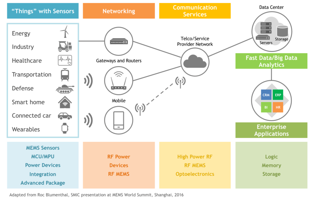
Figure 1: The IoT is not just about sensors. It conceals sensing, communications and computing ICs behind a seamless user experience.
In the future, a level 5 autonomous car, capable of full autonomy, will not just be dependent on advanced sensors, it will essentially be a self-aware server on wheels.
A recent McClean Report from IC Insights shows the underlying importance of ICs and their fabrication when it reveals IoT and automotive IC end-user markets to be the fastest growing areas over the 2017-2022 period with compound annual growth rates (CAGRs) of over 13 percent each. The two markets delivered $20.9 billion and $28 billion, respectively, in IC sales in just 2017.
A Marriage of Technologies
What holds devices together in the IoT and autonomous cars is not just sensing or machine-to-machine communication but a range of technologies. The march toward a networked society or Infrastructure of Things is indeed making strange bedfellows of a variety of fabrication techniques spanning materials and technology nodes.
In play are complementary metal oxide semiconductor (CMOS) processes for logic, bipolar CMOS (BiCMOS) or double-diffused MOS (DMOS) for power management ICs, DRAM for memory, 3D NAND for storage, wide bandgap devices such as silicon carbide (SiC), MOSFETs and gallium nitride (GaN) HEMTs Piezoelectric materials such as PZT, aluminum nitride (AlN) and scandium (Sc) doped AlN for RF filters and MEMS transducers as well as silicon germanium (SiGe) for RF ICs. If that were not enough, the devices in our key markets are currently manufactured with feature dimensions ranging from above 180nm down to below 28nm using older equipment handling 200mm wafers as well as newer machines for 300mm wafers.
Shared Challenges
Fabs face challenges in maintaining etch-depth and critical dimension (CD) control uniformity. Even the etched feature geometry or tilt can have a big impact on yield. These are all issues that must be dealt with at leading-edge technology nodes. For a 300 mm wafer, depending on die size, the outer 8 mm edge contains about 10 percent of the die, while the outer 2 mm edge has three percent of the die, making what happens at the edge an important influencer of overall productivity.
Edge discontinuities for material, temperature and electrical field during the etch process therefore have a significant impact on yield (figure 2).

Figure 2: The physics of what is happening on the wafer remains the same, whether fabs handle 200 mm wafers or 300 mm wafers.
While at the leading edge the discontinuities of the wafer can affect the bulk of the performance of CMOS, the same issues of etch-depth control, CD control and geometric control in terms of tilting effect the latest generations of MEMS, power and analog devices. That is because the physics of what is happening on the wafer is the same. Therefore, if we address challenges associated with the physics at advanced technology nodes, we can take those lessons and apply them to other applications.
Advanced Solutions For 200mm
Apart from technological challenges, fabs face the challenge of building capacity at a cost appropriate point. Existing fabs can now address the IoT and automotive markets at a price point that is well below adding equipment at the most advanced technology nodes.
Take for instance, the Versys® Kiyo45™ conductor etch product, which takes the lessons from Lam’s advanced 300mm experience and applies them to a 200mm wafer, resulting in increased repeatability, defect reduction, better wafer-to-wafer uniformity and higher throughput. Similarly, Lam’s VECTOR® PECVD system, which has been gaining market share in key 300 mm plasma enhanced chemical vapor deposition (PECVD) applications, was not initially introduced as a 200 mm tool. However, its success at 300 mm resulted in a pull from our customer base to make it available at 200mm. The 200mm version has since become a bridging tool when introduced last year.
The payback from applying advanced technologies at 200 mm do not end there. Power, mixed-signal applications, MEMS, CMOS image sensors and even some packaging applications, such as system in package (SiP), benefit from the introduction at 200mm of Lam’s latest generation deep silicon etch (DSiE) process module that incorporates learning and features from Lam’s 300 mm Versys® Kiyo45™ system and our Syndion® TSV etch tool (figure 3).

Figure 3: Pulling capabilities at 300 mm to apply them at 200 mm adds significant flexibility in a foundry environment.
A Tested Upgrade Strategy
There are many thousand 200 mm Lam Alliance® tools in the field today with many being in excess of 10 years old. Yet, they are still heavily utilized and Lam’s Reliant business continues to build both new and refurbished versions to support our customers. Lam’s customers can also upgrade older Alliance® tools with the advanced control system and software architecture of Lam’s 2300 platform. This Alliance® C upgrade also allows the tools to do things for which they weren’t originally designed.
Figure 4: By providing upgrades to older tools, Lam Research significantly improves the benefit of the customer’s assets.
Just by upgrading the control system architecture and the software, the Alliance C upgrade improves the timing and reproducibility on the tool. At one customer location, it resulted in a 46-percent standard deviation improvement in chamber-to-chamber CD with the process capability index (CPK) going up from 2.3 to 4.5.
The Alliance C upgrade also supports the addition of other upgrades such as throughput optimization (TPO), automatic preventive maintenance (AutoPM) and wet cleaning optimization (WCO). Whenever the process mix changes or a tool is repurposed, TPO software algorithms analyze and optimize the setup to improve tool performance. AutoPM runs a script to automate a large number of manual events and systematically and reproducibly bring the tool back online, thereby freeing up engineering resources to work on other systems. The WCO feature is software-guided cleaning guide that can be tailored to specific tool sets and provided in the customer’s local language. At customer sites, it has reduced labor time and unscheduled cleans.
Meeting Future Application Demands
Lam Research has built 300 mm technological expertise and a comprehensive range of products that meet specific needs, including those for piezoelectric and wide band gap materials, and high-performance deep silicon etch applications. The rapid growth in IoT and automotive markets is, however, driving demand for expansion in 200 mm capacity, often at nodes greater than 28 nm.
Lam is now addressing these challenges with cost appropriate solutions by leveraging advances made for 300 mm equipment and applying them through hardware and software upgrades of existing 200 mm product lines.