Line edge roughness (LER) can occur during the exposure step in lithography [1-2]. Similarly, etch and deposition process steps can leave a roughness on semiconductor surfaces. LER is a stochastic (or random) process, and it can cause device defects and lead to variability in device performance. This effect is more pronounced in advanced technology nodes beyond 5 nm, as there is less tolerance for these types of variations as device dimensions shrink. Process window optimization studies can help integration engineers study LER and develop process specifications to achieve their targeted yield. These types of process window optimization studies can be automated and expedited using SEMulator3D® process modeling.
Figure 1 (a-c) illustrates how to incorporate LER in process modeling using SEMulator3D®. LER can be modeled in SEMulator3D using an Edge Noise option in the Expose Material step (which is part of the Lithography Process Library). If LER is not included in the model, the patterned lines would be straight and devoid of any roughness [Figure 1 (d)]. These straight edges are unrealistic in a typical process flow. A more representative case of a typical patterned line with edge roughness is shown in Figure 1 (e), where Edge Noise was included in the model.
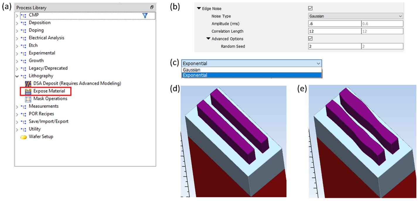
Figures 1: (a)-(c) Line edge roughness modeling options within SEMulator3D (left, top right and center). (d) A 3D model displaying straight lines with no line edge roughness. (e) A 3D model displaying lines with edge roughness using a Gaussian noise type setting (rms = 4 nm, Correlation length = 0.8 nm).
Next, we demonstrate how to simulate surface roughness. We start by using an etch step from the Process Library, and then choose the “Custom Loading Map” option in the Pattern Dependence model [Figure 2 (a)]. When the “Depth” option is selected, it allows the user to specify a Python module and class to determine the etch depth. This class option is required to have an associated array, and the values in this array control the etch depth at each point on the surface. [Figure 2 (b-d)]. The custom Python step can include entries to control the type of surface roughness formed. These entries include the roughness feature “count”, along with the mean and standard deviation of surface craters that comprise the surface roughness. The craters are polygon-shaped, and the number of vertices of these polygons can also be controlled by these entries.
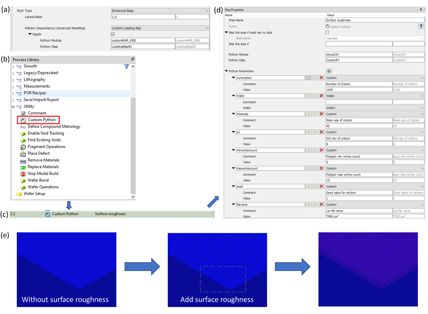
Figure 2: (a) In order to achieve surface roughness, an etch step with “Custom Loading Map” option can be used (upper left). (b-d) A custom Python step creates a .csv file that contains the etch depth at each point on the surface (center left and upper right figures) . (e) The resulting surface roughness (bottom figure), displaying a 3D model of surface roughness for various roughness settings) . Results for different values of the parameters are shown in Figure 3.
The surface roughness created by this process step will vary based upon the parameter values provided to the model. Figure 3 (a) displays 40 nm mean size roughness created during an etch step on a silicon dioxide surface. The values of the parameters can be chosen to improve the correlation between the model and actual wafer results [Figure 3 (a-d)]. Surface roughness often gets transferred to material etched or deposited later. As an example, surface roughness can lead to scumming[3] in photoresists, which in turn, can lead to shorts among lines (Figure 4).
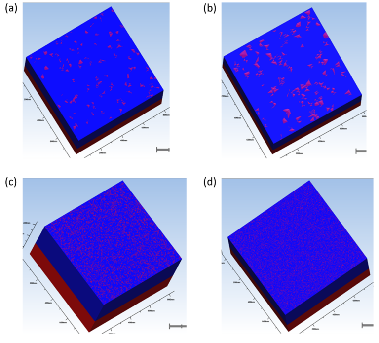
Figure 3: (a) (top left) Surface roughness achieved with a mean size setting of 40 nm and count of 1000. Different values were used for mean size and count of the craters that create the surface roughness in Figures (b) Size = 60, Count = 100 (c) Size = 10, Count = 10000 (d) Size = 4, Count = 100000 (Figure 3(b) is shown in the top right, and Figures 3(c) and 3(d) are shown in the bottom left and bottom right)
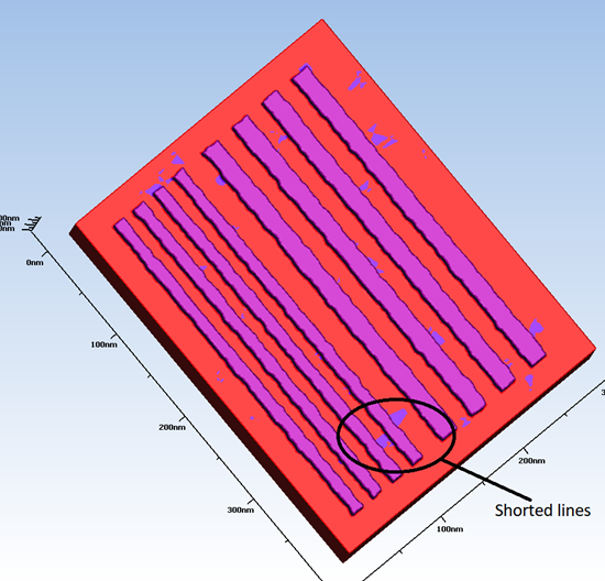
Figure 4: Surface roughness can get transferred to materials etched or deposited later. Here, the surface roughness has led to scumming, which in turn caused lines to get shorted.
Conclusion
Virtual modeling and calibration of LER can be used to minimize the impact of LER as semiconductor device dimensions decrease. Process window optimization studies in SEMulator3D can include LER effects, to improve both model accuracy and ultimately the calibration to measured results. Process window optimization modeling with LER can significantly improve the correlation between predicted yield and actual measured yield at advanced nodes, where sensitivity of these effects is most pronounced. SEMulator3D® has the capability to accurately model both line and surface roughness issues, to help engineers better understand and control the consequences of LER during advanced device manufacturing.
References
[1] Lin, Q., Black, C. T., Detavernier, C., Gignac, L., Guarini, K., Herbst, B., … & Sanchez, M. I. (2003, June). Does line-edge roughness matter? : FEOL and BEOL perspectives. In Advances in Resist Technology and Processing XX (Vol. 5039, pp. 1076-1085). SPIE.
[3] Sobieski, D., Wise, R., Pan, Y., Fried, D., Yu, J., & Shamma, N. (2019, March). EUV line-space pattern defect mitigation simulation using Coventor SEMulator3D to enable exposure dose reduction. In Advanced Etch Technology for Nanopatterning VIII (Vol. 10963, pp. 90-98). SPIE.