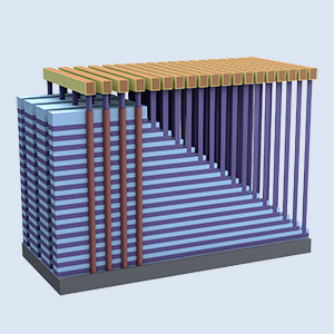
The industry’s transition to 3D NAND is being driven by several important advantages, including its ability to deliver higher capacity with a lower cost per bit. These vertical architectures rely more on advances in deposition and etch than lithography to create critical device structures, raising new manufacturing issues. Addressing these challenges is the focus of a recent article by Lam’s Harmeet Singh in Solid State Technology.
Since its introduction several years ago, 3D NAND has become a mainstream technology because of its ability to increase bit density in memory devices. Its adoption has been accelerated by advances in the underlying manufacturing processes that are enabling 3D architectures and lowering the cost per bit. With all its advantages, however, the overall complexity and capital intensity of 3D NAND manufacturing add significantly to the challenges fabs are facing in terms of process control, yield, and economics.
Market and Technology Drivers for 3D NAND
The main impetus for 3D NAND was the recognition that planar technology was approaching the end of its physical limits to deliver higher densities and a lower cost-per-bit. Past advances in conventional planar NAND technology have primarily been driven by physical scaling, where lithography capabilities determined just how many memory cells could fit within a given die size. Using multiple levels of charge within each cell by going from single- to multi-level cell designs has also enabled increased bit densities. However, these improvements typically have come at the expense of speed because of the need to differentiate between the multiple levels of charge. In addition, since the individual memory cells for these designs lie in a horizontal plane, scaling is still ultimately limited by lithography. Other challenges in scaling 2D NAND beyond the 15 nm node include cell-to-cell interference, unscalable dielectrics, and electron leakage.
To address these issues, 3D NAND fundamentally changes the scaling paradigm. Instead of traditional X-Y scaling in a horizontal plane, 3D NAND scales in the Z-direction by stacking multiple layers of NAND gates vertically. This allows more cells to be packed into the same X-Y space (planar area) on the die without shrinking dimensions horizontally. By easing cell size requirements, triple- and even quadruple-level cell designs are possible. As such, 3D NAND offers a significant increase in bit density over planar NAND.
Unlike planar NAND, where scaling is primarily driven by lithography, 3D NAND scaling is enabled by advances in deposition and etch processes. An incredible level of precision and repetition is required in defining complex 3D structures with extremely high aspect ratio (HAR) features. Achieving success with 3D NAND requires innovative deposition and etch solutions that minimize variability.
Continue reading at Solid State Technology.
Learn more about 3D NAND in our Tech Brief: Memory “Grows Up” with 3D NAND.
