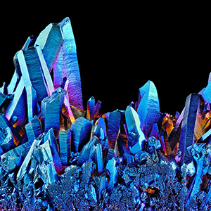
More than most industries, ours is identified with a single element, silicon. Consider the self-adopted naming conventions of all the places that want to be recognized as members of the club—Silicon Valley, Silicon Beach, Silicon Forest and so on. Silicon wafers are fundamental in manufacturing the electronic “chips” that pervade almost every aspect of our lives. New applications in IoT, wearable and mobile devices, self-driving cars, cloud computing, 5G communication networks, and more, practically guarantee that demand for wafers will continue to grow at an accelerating rate. SEMI, the semiconductor equipment manufacturers’ industry association, recently announced that 2018 shipments of silicon wafers had set a new record of more than 12 billion square inches, up 8% from the previous year. Revenues for the year totaled $11.38 billion, up 31% from the previous year and exceeding $10 billion for the first time ever. But wafers are not the only place silicon is used and they are not even close to the largest consumer of silicon. Construction (sand and concrete) followed by steel and aluminum are by far the largest. There are smaller applications for silicon that are also critical, such as solar energy and specialty parts for semiconductor manufacturing equipment.
Sand to Wafers…
Fortunately, there is no shortage of raw material. Silicon is the second most common element in the earth’s crust, comprising about 26% and exceeded only by oxygen at 49%. But silicon does not occur naturally in the pure form needed for electronic applications, for which it must contain less than one in a billion non-silicon atoms. The starting material really is sand. Not just any sand, but silica sand, specially quarried for this purpose and having concentrations of quartz (silicon dioxide) as high as 95%.
Purification starts by heating the sand with a reducing agent, carbon, to produce carbon monoxide and silicon. The product of this process, known as metallurgical grade silicon (MG-Si), may be as much as 99% pure. Additional processing is completed until ultrapure electronic grade silicon (EG-Si) is obtained.
In addition to being very pure, the silicon used in integrated circuits must also consist of a single perfect crystal. That crystal is grown by placing a small seed crystal in contact with the surface of a reservoir of molten silicon. As the seed crystal is slowly “pulled” up away from the melt, silicon atoms deposit on the bottom surface, perfectly matching and extending the crystalline lattice of the seed. The result is a large cylindrical “boule.” The boule is sliced into wafers less than a millimeter thick, and finally, the wafer surfaces are polished atomically smooth and the edges are shaped to remove cracks and chips.

…And More
Silicon is used in many applications other than semiconductor wafers. Most MG-Si is used in metallurgical applications, where it is frequently alloyed with metals like aluminum and iron to enhance certain properties. Electronic grade silicon, in polycrystalline (“poly”) and amorphous (glass-like non-crystalline) forms is used in photovoltaic (solar) cells and thin film transistors. Poly is also used to form component structures, such as transistor gates, within integrated circuits.
Ultrapure silicon is also used to make parts for semiconductor manufacturing tools. For example, dielectric etch systems, which remove insulating material used to isolate the conductive components of an integrated circuit, contain critical parts made of high purity silicon. These tools use a process known as reactive ion etching (RIE), which bombards the wafer surface with charged particles (ions) to remove material. The ions are created in a plasma generated by an electromagnetic field applied to a low-pressure gas that is introduced into the process chamber above the wafer. Silicon is an ideal material for critical parts located near the wafer and exposed to the plasma, since it avoids the possibility of contaminating the wafer by redepositing foreign material etched from non-silicon chamber components.
One of the most critical aspects of etch system performance is maintaining the uniformity of the etch process across the wafer, which in turn requires maintaining the uniformity of the plasma. For example, the “showerhead,” through which the etch gas enters the process chamber, contains thousands of holes that must be precisely sized and located to distribute the gas evenly over the wafer. Uniformity can be especially difficult to maintain near the edge of the wafer, where there are electrical, thermal and chemical discontinuities. Surrounding the wafer with an edge ring also made of silicon can significantly reduce these discontinuities. Another critical component best made of silicon is the plasma confinement ring that helps to keep the plasma concentrated over the wafer.

Silicon, which is very hard and brittle, is a challenging material to work with. Recognizing the criticality of these components, Lam Research has invested heavily in developing the specialized capabilities required to manufacture them. Silfex, Inc. (a division of Lam Research) is the world’s largest provider of high purity custom silicon components and assemblies. Silfex has state-of-the-art material growing and CNC machining centers, as well as automated cleaning systems in which final parts are processed and packaged within a cleanroom environment to meet industry requirements. The manufacturing processes are designed around producing high precision silicon parts, contributing to the success of Lam’s plasma etch systems.