Imagine being able to deposit a film of material just a few atomic layers at a time. As impossible as that sounds, atomic layer deposition (ALD) is a reality. In fact, it’s being used in an ever-increasing number of applications as an extremely precise and controllable process for creating thin films. Together with its etch counterpart – atomic layer etching (ALE) – ALD is enabling the use of new materials and three-dimensional designs in advanced chip manufacturing. In this Tech Brief, we’ll take a closer look at this important atomic-scale process.
Chemical Vapor Deposition
ALD is actually a type of chemical vapor deposition (CVD), one of the most common methods of producing thin films during chip-making. In CVD, gaseous “precursor” chemicals flow into a process chamber that contains the silicon wafer. These precursors react on the wafer surface, forming the desired film along with byproducts that are removed from the chamber. Plasma-enhanced CVD (PECVD) uses a plasma to lower the deposition temperature while maintaining good film quality and high deposition rates. This is an important advantage since some CVD processes involve higher temperatures than can be tolerated by materials used in today’s advanced semiconductors. However, the PECVD process is “soupy” – precursors, plasma, byproducts, and other molecular fragments and species are all floating around in the chamber, making it difficult to control film deposition to the atomic scale.

The graphic shows the "PECVD Process" flow in four stages:
- Precursors flow into chamber
- Plasma creates mix of species
- Species absorb on the surface and react
- Film grows and byproducts are released
Atomic Layer Deposition
The secret to gaining improved control was to split the deposition process into half-reactions, each of which can be well-controlled. The ALD process starts by flooding the reaction chamber with a precursor that coats (or “adsorbs” onto) the exposed surface of the wafer. This process is called self-limiting because the precursor can only adsorb onto exposed areas; once all those are covered, the adsorption stops. A second gas is then introduced and reacts with the precursor to form the desired material. This second step is also self-limiting: once the available precursor sites are used up, the reaction stops. The two steps are repeated until the desired film thickness is obtained.

The graphic displays the "ALD Process (SiO2 Example)" in five steps.
- The Si surface (empty)
- Si Precursor
- The Si Precursor settles
- O2 Plasma is introduced
- SiO2 is added
There are a couple of ways to divide the steps. In one technique known as spatial ALD, the wafer is moved between different locations and exposed to a different precursor at each. Another approach is to hold the wafer in one place and alternately introduce/remove precursors into the chamber. Known as temporal ALD, this method enables the wafer to be processed in a more symmetric environment, improving process results such as better critical dimension (CD) range control.
ALD Advantages
ALD offers a number of advantages, all of which arise from the self-limiting, sequential reactions. First, while deposition is not exactly a single atomic layer per cycle, film thickness is well controlled and excellent uniformity can be achieved across the wafer. Perhaps even more importantly, ALD creates layers that conform extremely well to the wafer topography, with identical film thicknesses deposited on the tops, sides, and bottoms of device features. This high conformality is a critical capability for high-aspect-ratio and 3D structures. Lastly, surfaces created by ALD are atomically smooth, with well-controlled chemical composition.

The graphic depicts examples of poor and good deposition.
Poor uniformity shows uneven deposition (looks like rolling hills). Poor conformality shows varying thicknesses around edges. Poor surface smoothness shows ragged smoothness on the surface.
Good uniformity and good surface smoothness shows a clean even line on the surface. The same with good conformality -- an even thickness around all edges.
Applications
The ALD process is capable of creating both dielectric (insulating) and metal (conducting) films, depending on the choice of precursors. Its many advantages have led ALD to be used in several applications, and here we take a brief look at some of these.
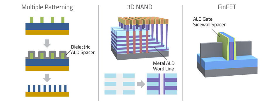
Self-Aligned Patterning: ALD plays a key role in self-aligned multiple patterning, which is used to form patterns smaller than can be produced with current lithography technology. In this technique, a thin spacer is deposited on pre-defined features. This spacer film must be highly conformal and very uniform as it will eventually define the critical dimensions of the final pattern.
3D NAND: The three-dimensional structures in 3D NAND memory devices require a high degree of process variability control. ALD is well suited for this and is used to form dielectric films on the sidewalls of memory holes. Metal ALD is also used for the word line fill in replacement-gate schemes, which require lateral deposition that completely fills narrow, horizontal features.
FinFET: The thin gate sidewall spacers in finFETs must be formed with extremely uniform thickness and no pinholes. ALD is an excellent way of depositing this layer, which separates the control gate from the three-dimensional fin structure.

There are three depictions.
Multiple Patterning: A thin spacer (Dielectric ALD Spacer) covers predefined features, which look like pillars.
3D NAND: A three dimensional structure that looks like the skeleton of a skyscraper. A cut out shows how Metal ALD Word Line to fill in replacement-gate schemes.
FinFET: A thin ALD Gate Sidewall Spacer appears in the middle of the fin.
Future Applications
The uses for ALD continue to grow. For example, one promising application is selective area deposition, which leverages inherently selective films. Researchers are currently developing ways to deposit metals and dielectrics in very specific locations – essentially creating a different patterning method. For the first time, selectivity is the most important film property and will be essential for integration at the 5 nm to 3 nm technology nodes. ALD is also being explored as a means to improve overlay control, or how precisely a new pattern can be aligned over an existing pattern. Any offset or misalignment to underlying electrical contacts can reduce conduction and negatively impact chip performance.

Selective Area Deposition is shown. The graphic shows how the film can be deposited around the edges of the design or within the design elements themselves (lines, pillars).
Looking ahead, we expect atomic layer processing to play an increasingly important role in advancing semiconductor manufacturing as these and other applications develop. Proven as a key enabling technology, ALD continues to evolve for use in challenging new structures and scaling strategies as they are integrated into next-generation devices.