From PCRAM and MRAM to RRAM and more, there’s a whole new alphabet soup of memory technologies making their way to the fab. Fueling this development are technology advances in gaming and mobile products and the growth of cloud computing – important applications that are stretching the capabilities of today’s mainstream memory technologies. For example, gaming requires extremely fast primary (main) memory and high-capacity secondary (storage-class) memory to maneuver massive quantities of graphics data quickly enough such that data handling is imperceptible to the user. After all, no one wants an unexpected pause at a critical moment in their game. In cloud computing, the big payoff is being able to access vast amounts of data through the internet, rather than having to store data directly on our personal devices. Here as well, speed is paramount since we don’t want to wait a single nanosecond longer than necessary.
Closing the Memory Gap
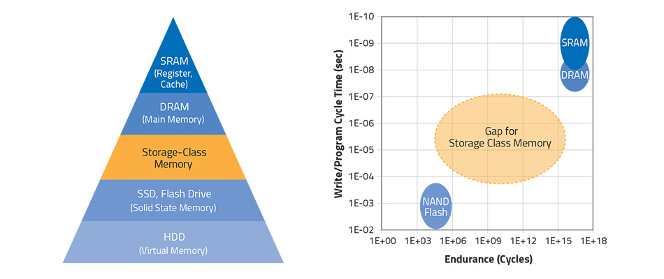
As explained in our primer, “Tech Brief: Much Ado about Memory,” DRAM and NAND flash are the most common technologies currently in use for fast main memory and slower storage-class memory, respectively. To meet increasing performance requirements – including improvements to memory speed, capacity, power usage, and scalability – several new technologies are being explored.
Most of these new disruptive memory technologies are non-volatile, meaning they do not require power to retain data, and generally target storage-class applications. Since they are also random access, they are faster than NAND flash, which is currently used for many storage applications. In addition, these relatively large memory components can be built in the back end of the line (BEOL) of the chip. Thus, they avoid further crowding of components like transistors that are built in the front end of the line (FEOL). Since they are fabricated on different levels than other types of memory, they provide a significant scaling advantage.
Phase Change RAM (PCRAM)
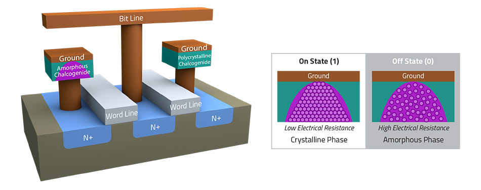
Because PCRAM – also called phase change memory (PCM) – offers performance on par with DRAM (random access, bit-addressable, and bit-alterable), it is being considered for main memory as well as storage-class applications. PCRAM technology makes use of the property of chalcogenide glass (Ge2Sb2Te5, or GST) to change states under the influence of heat, hence the term “phase change.” An electric current is passed through a heating element (resistor) to switch the GST between its polycrystalline (low resistance) and amorphous (high resistance) states. The difference in resistance correlates to the data value (“0” or “1”) stored in the cell.
Manufacturing these devices is tricky, particularly for the etch steps. GST’s three materials – germanium, antimony, and tellurium – must be etched at the same time. However, they have different etch rates, and differences in material removal can lead to sidewall damage and profile bowing of the device feature. Another challenge is cleaning the post-etch GST residues without causing collapse of the high aspect ratio structure or a thick layer of oxide to form around the GST. An oxide layer would replace much of this conductive material and impact device performance by reducing the signal-to-noise ratio. As device features shrink, the area for the GST decreases while the amount of damaged area remains the same (percentage of the damaged area increases). Eventually, the electrical signal can no longer be reliably detected because there is not enough GST, and solutions are being developed to address this issue.
Magnetoresistive RAM (MRAM)
MRAM’s speed and storage capabilities also make it suitable for both main memory and storage-class applications. One type of MRAM gaining attention is spin-transfer torque MRAM (STT-MRAM). STT in MRAM makes use of an electron’s intrinsic spin to reduce the current required to reach the threshold voltage (level needed to activate a cell), thereby saving power. It is fast enough to compete with SRAM (static RAM) for cache memory applications. Also, SRAM is a behemoth, taking up roughly 50% to 80% of the space in a computer’s microprocessor or central processing unit (CPU). Being able to build MRAM into the BEOL levels of a chip offers a huge scaling advantage over large SRAM arrays that are built into the FEOL levels.
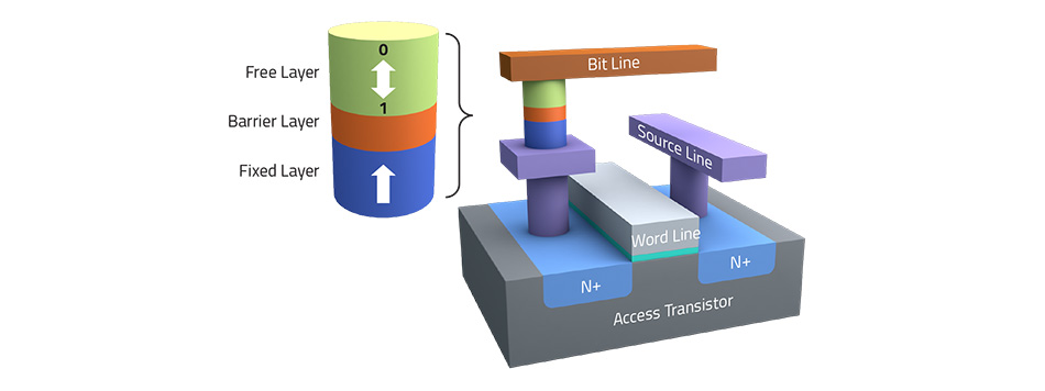
MRAM uses magnetic storage elements rather than conventional electric charges to store data. Each cell consists of two magnets: one that is stationary, and one that can flip. When the magnets are parallel to each other, resistance is low; when the second magnet flips and reverses direction, the resistance is high. Similar to PCRAM, the change in resistance correlates to a “0” or “1” data value.
As with PCRAM, the etch steps for MRAM devices are among the most challenging in the manufacturing process. The cobalt-iron (CoFe) and cobalt-iron-boron (CoFeB) magnetic layers are difficult to etch because they don’t readily form volatile compounds with plasma gases so they can be removed. Thus, these processes need to bombard the wafer surface with ions (sputtering) to remove material. This creates tapered profiles with residue near the base instead of vertical profiles, an effect that limits how close together device features can be placed. If the bases of tapered features are too close, an electrical short may result. One approach to correcting this problem is ion beam etching, which controls the angle of ions hitting the surface by tilting and rotating the wafer to target material removal at the base.
Adding to the issues, the magnesium oxide (MgO) tunneling barriers that switch the magnets are easily damaged. Depositing a layer of material around the barriers (“encapsulation”) immediately after the etch step protects them from corrosion and limits their exposure to air, preventing MgO from forming unwanted magnesium hydroxide (MgOH).
Resistive RAM (ReRAM or RRAM)
For mobile electronics, RRAM is being explored as a future replacement for NAND flash, which at some point may not be able to deliver sufficiently high storage capacity at low cost. RRAM is faster than flash, being both random access and bit-alterable, making it a good choice for high-performance storage-class applications. It also has promise in both cross-point and 3D vertical architectures, which enable achieving greater bit density (higher storage capacity).
Similar to PCRAM, RRAM places a material that changes resistance between two electrodes. An electric field or heat causes a change in the material’s ion distribution, which provides a measurable change in resistance that can be used as a signal.
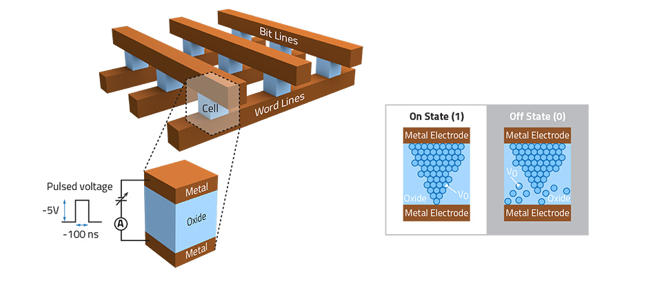
Like MRAM, RRAM has some non-volatile materials that need to be etched, including copper telluride (CuTe) and copper geranium (CuGe). Since copper-based materials are difficult to etch, alternate manufacturing solutions are needed for these designs. One approach is to change the architecture so that a damascene process can be used. Damascene strategies address this issue by first depositing, then etching a dielectric material. Next, the copper material is deposited, thereby avoiding the challenge of having to etch it. Another concern is exposure of highly reactive materials like copper-based films to air, which can lead to oxidation and change their properties. Controlling exposure is critical for many of these materials, and encapsulation is used for these devices much like its use for MRAM.
Disruptive Innovation Transforming Electronics
Looking ahead, the industry is searching out even more approaches beyond these new non-volatile memory types. New solutions are needed because the latest CPUs are so fast that data transport is now impeding overall chip speed. To improve speed and reduce power usage, one idea is to integrate memory and logic on a single chip, while another is to design a more data-centric layout of logic and memory components. Though both concepts hold promise, there are significant design and manufacturing issues to address. To increase storage without losing speed, one option being explored is hybrid memory cubes that place DRAM cells closer together to shorten the data transmission pathway.

Another fascinating area is neuromorphic computing – modeling CPUs after the function of the human brain and its nervous system. Here, in addition to design challenges, managing energy consumption will be critical. While the human brain uses only about 2-20 Watts, a computer today would require about 20,000,000 Watts to perform brain-like functions! While a neuromorphic architecture would consume much less power, it would only be suitable for certain activities. CPUs use a discrete “1” or “0” (on or off) logic, which is extremely accurate. Neuromorphic values would be scaled and need around 75% or 80% accuracy for the signal to be recognized. Consequently, this area is still being defined and explored.
With this innovation, the world of computing and its wide array of supporting memory devices may operate quite differently in the not too distant future. Fortunately for all of us who enjoy and rely on electronic products, all we may notice of these revolutionary changes is the lightning fast, powerful capabilities they’re sure to bring.