We often hear the word “inflection” used in the semiconductor industry, but what does it mean? In general, inflection refers to a point of change. In mathematics, for instance, an inflection point is the place where a curve reverses direction. In terms of technology, an inflection is often identified as a new approach that leads to significant improvement or disruption.
Inflections in Technology
A good example of an inflection is what happened when television first became available to the average U.S. consumer back in the 1950s. Major change was required for the television to become a form of mass media, including the development of a supporting infrastructure through a host of related businesses. These included not only TV manufacturers and installation/repair services, but also the creation, production, and broadcasting of shows. Likewise, the growth of internet usage in the early 2000s was an inflection in that it fueled innovation such as new content development tools, led to new businesses like service providers, and ultimately contributed to the widespread and rapid sharing of information.

Inflections in the History of Chip-Making
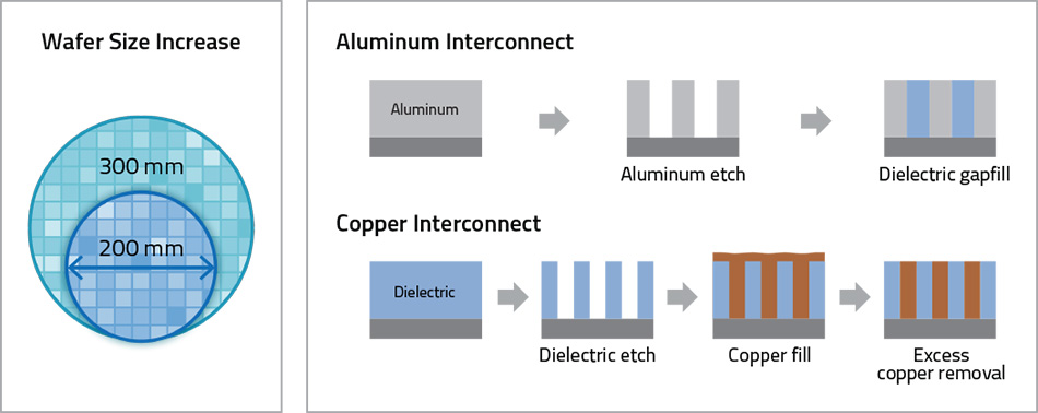
The continued extension of Moore’s Law is due in large part to inflections in the semiconductor world. One simple example of an industry inflection is the wafer size transition from 200 mm (~8 inches) to 300 mm (~12 inches) that occurred during the early 2000s. By using 300 mm-diameter wafers, manufacturers could produce more than twice as many chips per wafer. However, this size change involved solving many technical challenges, including the redesign of manufacturing equipment, new process capabilities, and a greater reliance on robotics to accommodate the larger wafers. As a result, it was several years before 300 mm wafers were commonly used in high-volume production.
The term “technology inflection” typically describes a revolutionary change in a wafer processing scheme or device architecture. These changes, in turn, drive the development of new semiconductor manufacturing capabilities. A classic case is when interconnects (the tiny wires that electrically connect components of a chip) switched from aluminum to copper in the late 1990s. Copper has higher electrical conductivity than aluminum, so chips made with copper interconnects can run faster and use less power. However, it turned out that copper was much harder to etch than aluminum, so fundamentally new processing schemes had to be developed. In this case, instead of etching the metal and filling the gaps with an insulating dielectric film, copper interconnects required etching the dielectric film and then filling the gaps with metal. Integrating the new schemes was challenging and took several years to achieve industry acceptance.

A box on the left says "Wafer Size Increase" and has a 300 mm wide wafer and a 200 mm wide wafer. On the right the box a label on top says "Aluminum Interconnect." A series of three images below show a block of aluminum, then aluminum etch, and finally dialectic gapfill. On the bottom under the label of "Copper Interconnect" are four images show its progression: dialectic, then dialectic etch, then copper fill, and finally excess copper removal.
Today’s Multiple Inflections
The semiconductor industry today is in the unusual position of facing multiple technology inflections at the same time. Incremental, evolutionary scaling strategies are coming to an end, and revolutionary approaches are needed to keep Moore’s Law on track, thus providing consumers with smaller, faster, and lower power devices. Here are some of the inflection points that are currently in progress.
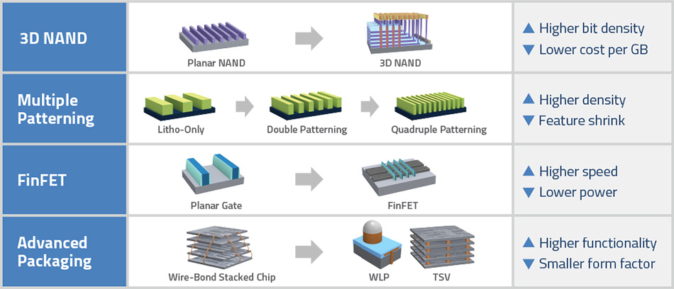
3D NAND – NAND flash, a popular type of memory used for example in mobile devices, has traditionally been made using two-dimensional (2D), or planar, methods. To squeeze in more memory capacity without having to shrink feature dimensions, 3D NAND builds up, or vertically. This three-dimensional memory structure is so different from planar NAND that new fabrication methods are being developed.
Multiple Patterning – Used throughout the manufacturing process, patterning is the set of steps that transfers chip designs onto wafers. Today those designs often have features smaller than can be created with a single patterning cycle using current lithography capability. By repeating lithography, etch, and deposition steps, multiple patterning techniques (including double, triple, and even quadruple patterning) create the smaller, more closely packed features needed to continue scaling.
FinFET – The planar transistor has been the foundation of the semiconductor industry for decades, with each generation having smaller features than the last. With scaling for advanced devices beginning to approach physical limits, new architectures such as vertical transistor structures are needed. FinFETs use tall “fin-like” structures to achieve higher chip speed and most importantly, lower power.
Advanced Packaging – Packaging involves enclosing the chip for protection and providing external connections for signals and power. Packaging approaches such as chip-level and wafer-level packaging (WLP) are being pursued to reduce form factor and increase functionality. One technique uses through-silicon vias (TSVs) to connect stacks of chips—yet another 3D scaling strategy.

There are four rows.
Row 1: 3D NAND. Icons show the progression from Planar NAND to 3D NAND. The process has higher bit density and lower cost GB.
Row 2: Multiple Patterning. Icons show the progression from Litho-Only to Double Patterning to Quadruple Patterning. The process has higher density and lower feature sink.
Row 3: FinFET. Icons show the progression from Planar Gate to FinFET. The process has higher speed and lower power.
Row 4: Advanced Packaging. Icons show the progression from Wire-Bond Stacked Chip to WLP and TSV. The process has higher functionality and smaller form factor.
What Changes Does the Future Hold?
Looking ahead, future inflections will continue to focus on addressing scaling challenges for next-generation device nodes. Technologies being explored include hybrid patterning schemes, new logic gate structures and materials, novel memory architectures, and alternate approaches to interconnect metallization.
Collaboration across multiple disciplines will be a key factor in achieving success for both current and future inflections. Fortunately, our industry has an amazing capacity to come together and develop extraordinary technologies. And who isn’t excited about the new electronic products that these inflections will enable?