In a two-tier 3D NAND structure, the upper and lower channel hole profile can be different, and this combination of different profiles leads to different top-down visible areas. The visible area is the key metric to determine whether the bottom SONO (silicon-oxide-nitride-oxide) layer can be punched through and ensure that the bit cells connect to the common source line.
Performing channel hole profile splits on a silicon wafer is expensive and can be difficult or impossible to perform in real life. In this article, we will discuss the development of a virtual model containing two tiers of 64 oxide-nitride stacks and perform a virtual DOE (Design of Experiments) on the upper and lower channel hole profiles to understand their impact on the SONO punch area. This example will demonstrate how virtual fabrication can help identify process margins and provide guidance for inline process spec control.

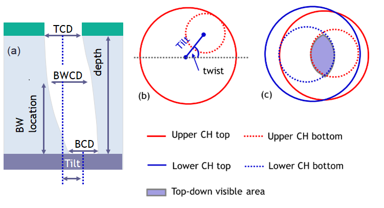
Figure 1: Schematic of a typical channel hole profile, with (a) cross sectional view, (b) top view, (c) overlap and visible area.
Figure 1 (a) shows a cross-sectional view of a channel hole profile with the major profile variables identified: top CD (TCD), bottom CD (BCD), bow CD (BWCD), and bow location (BW location). Figure 1 (b) shows a top view of the channel hole, showing the tilt distance and twist angle. Figure 1 (c) shows the overlap of the upper and lower channel holes; the overlapping visible area, which is a metric of the SONO punch process window, is shown in blue.
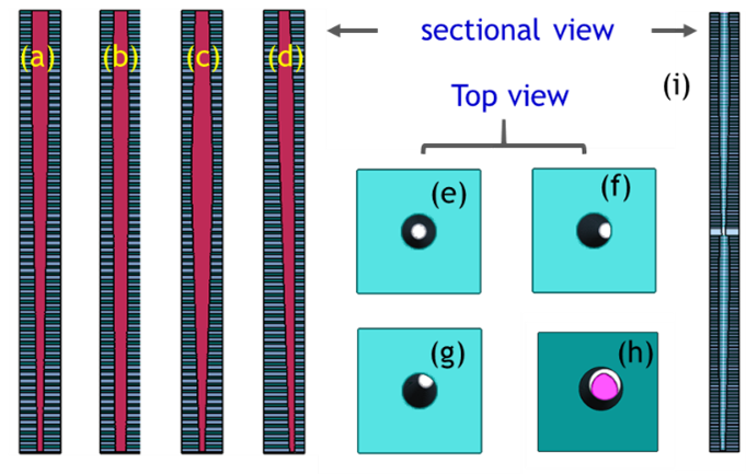
Figure 2 displays the CH profile generated using SEMulator3D® software. The top CD, bottom CD, bow CD, bow location, tilt distance, and twist angle can be defined by the user in the model. Figures 2 (h) and (i) show the top and cross-sectional view of the two-tier channel structure.

Figure 2: Different channel profiles showing (a) baseline, (b) small top CD and large bottom CD, (c) larger bow CD and lower bow location, (d) tilt, (e) baseline top view, (f) top view with tilt, (g) top view with tilt and twist, (h) top view with both tiers of the visible area, (i) two tiers of CH.
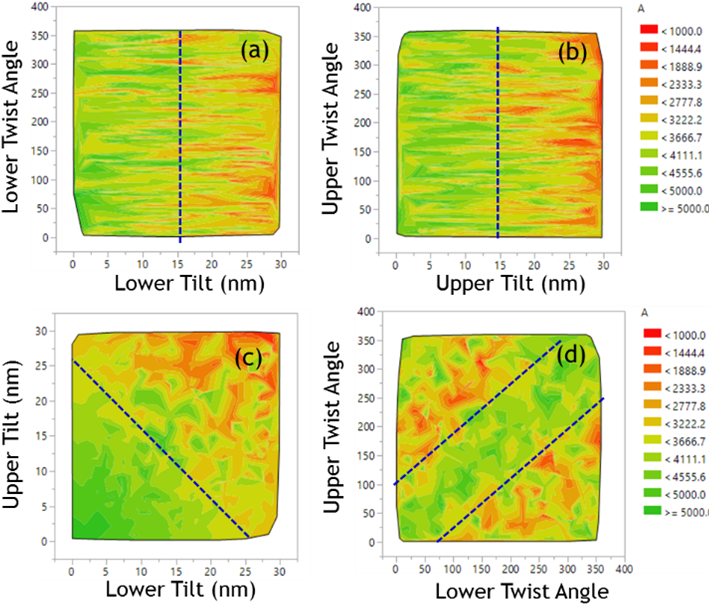
During the DOE, we fixed the top CD, bottom CD, bow CD, and bow location, and only varied the tilt distance and twist angle of both the upper and lower channel for simplicity. Based upon the DOE results, a smaller lower and upper tilt distance results in a larger visible area (Figures 3 (a) (b) (c)). The maximum visible area can be obtained when the upper twist angle and lower twist angle are close to each other in value (Figure 3 (d)). These results make intuitive sense and confirm the underlying logic of the virtual experiments.

Figure 3: Visible area contour with respect to tilt distances and twist angles.
To gain insight into the relationship between the visible area and the input variables, we created three new independent variables: lower tilt distance, delta tilt distance (the difference between upper tilt and lower tilt), and delta twist angle (the difference between the upper and lower twist angles).
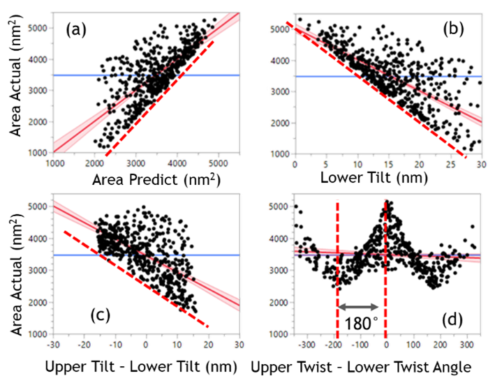
A regression analysis was then performed to generate leverage plots that display the relationship between these variables and the resulting visible area. Figure 4 (a) shows the predicted visible area vs. the actual visible area. Figure 4 also displays the visible area vs. the lower tilt distance (b), delta tilt distance (c), and delta twist angle (d).

Figure 4: Visible area leverage plot with respect to tilt distance and twist angles.
In the worst case, the visible area will decrease by about 150 nm2 when the lower tilt distance increases by 1 nm. Also, the visible area will decrease by 70 nm2 when the delta tilt distance increases by 1 nm. The analysis shows that if lower tilt is unavoidable, having the upper tilt grow less slowly than the lower tilt will result in a larger visible area. (In other words, upper tilt distance control is more important than lower tilt distance control.)
The visible area has no correlation with a single twist angle but is strongly correlated with differences in the upper and lower twist angle (the delta twist angle). The closer the twist angles are to each other, the larger the visible area will be. If twisting is unavoidable, ensuring twist in the same direction can mitigate negative impacts. In a real fabrication process, this may require using the same etch tool, chamber, and recipe when etching the lower and upper channel holes.
In this virtual DOE, only four variables were used to demonstrate the capabilities of virtual fabrication. More variables (such as various CDs) can be added to the model to conduct a more complicated DOE or execute a more well-rounded study.
This methodology can also be used as a feed forward control system. For example, if the bottom tier has already been fabricated on a Si wafer, then the twist, tilt, and CD information of the bottom tier could be measured. Based on the metrology distribution of the bottom tier, virtual fabrication could then help determine the corresponding specifications required at the top tier to help produce a two-tier structure with a larger visible area.
From this example, we can see that virtual fabrication is a powerful tool to perform sensitivity analysis and provide guidance for inline process spec control.
Qingpeng Wang is a semiconductor process & integration engineer for the Semiverse Solutions group at Lam Research