Month Year
| Su | Mo | Tu | We | Th | Fr | Sa |
|---|---|---|---|---|---|---|
Month Year
| Su | Mo | Tu | We | Th | Fr | Sa |
|---|---|---|---|---|---|---|


 |Sep 26, 2023|
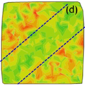
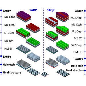
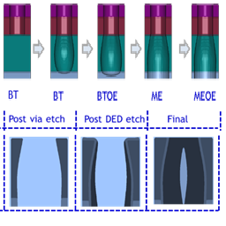
Virtual fabrication is a powerful tool to perform sensitivity analysis and provide guidance for inline process spec control
 |Sep 22, 2022|
With continuous device scaling, process windows have become narrower and narrower due to smaller feature sizes and greater process step variability [1]. A key task during the R&D stage of...
 |Feb 11, 2022|
Design of Experiments (DOE) is a powerful concept in semiconductor engineering research and development. DOEs are sets of experiments used to explore the sensitivity of experimental variables and...