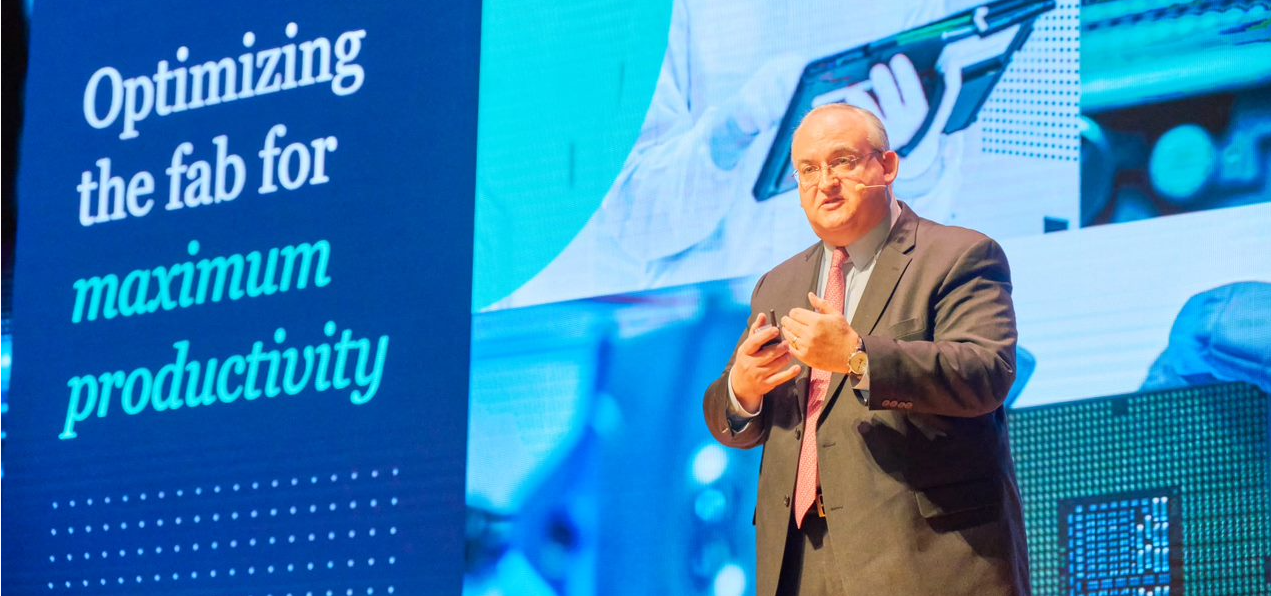
SEMICON Korea 2023 kicked off with a keynote speech, “Accelerating Innovation – From Lab to Fab,” delivered by Pat Lord, EVP of Lam Research's Customer Support Business Group and Global Operations. Pat shared how Lam is accelerating innovation throughout the value chain – from R&D process development in the lab to optimizing productivity in the fab – to deliver on our promise of technological advancement.
Lam was a platinum sponsor of SEMICON Korea 2023 (Feb 1-3, Seoul) and the sole sponsor of the SEMI Technology Symposium (STS). Alongside Pat, several of Lam’s experts spoke at the SEMI Technology Symposium, Workforce Development (WFD), and Diversity, Equity and Inclusion (DEI) programs.
Scores of local and global semiconductor companies from various sectors, including materials, parts, and equipment, participated in this event. Here is a recap of the main presentations from Lam Research participants at SEMICON Korea 2023.
Keynote Speech by Pat Lord on “Accelerating Innovation – From Lab to Fab”
From the abstract of Pat Lord's speech: The past several years have highlighted the critical role that technology plays in the world. It’s also highlighted just how high the stakes are for delivering that technology. The world expects more advanced technology, and gaps in meeting the demand have repercussions across the global economy. As an industry, we need to act with mutual collaboration to drive speed to solution. In this talk, Lord shares how Lam is focused on accelerating innovation throughout the value chain – from process development in the lab to optimizing productivity in the fab – so that we can deliver on the promise of technology advancement.
SEMI Technology Symposium (STS)
The SEMI Technology Symposium, an international technology symposium showcasing the latest developments in the chipmaking industry, was held concurrently with SEMICON Korea 2023 on February 1 and 2. Industry experts, including Lam’s own, gathered to share their insights to address the industry's challenges and discuss its future.
In S2. Advanced Materials and Process Technology session on the first day of SEMICON Korea 2023, Benjamin Eynon, senior director marketing, talked about EUV dry resist for continuous scaling of semiconductor devices. Introducing the key advantages of dry resist processing over wet resist processing, Eynon introduced Lam Research’s revolutionary technique of applying both EUV photoresist and developing latent images in the photoresist using dry technologies instead of the wet spin coating and development that have been in use over the last three decades.
In S3. Device Technology session, Benjamin Vincent, Senior Manager Coventor, gave a presentation titled, “A New 3D DRAM Si Nanosheet Architecture – Virtual Semiconductor Processing for Technology Pathfinding.” Since the introduction of 3D-NAND memory technologies during the last decade, he said the logic industry has also been preparing its own transition to three-dimensional devices by adopting nanosheet transistors. He also introduced innovative patterning designs and concepts for new semiconductor architectures as well as a new DRAM architectural concept developed using SEMulator3D® process simulation, which is based on the gate-all-around (GAA) nanosheet transistor.
In S4. Plasma Science and Etching Technology session, Thorsten Lill, VP Technology, gave a speech “Recent Progress in High Aspect Ratio Patterning for Memory Devices.” 3D memory devices have seen tremendous growth over the past few years due to increasing demands for the digitalization of the economy. Regarding this, he used experimental data and computational simulation to investigate the mechanisms of high aspect ratio dielectric etch in conventional and novel process regimes. In addition, Lill mentioned that individual etch and deposition module optimization and deposition and etch co-optimization(DECO) could provide new opportunities to overcome the oxide-nitride-oxide-nitride(ONON) and mask patterning barriers. He also introduced a sacrificial liner approach to prevent top critical dimension(CD) enlargement at deeper etch depths.
In S4 session, David Haynes, Vice President, presentd “Deep Reactive Ion Etch – Enabling Advanced Specialty Technologies and Packaging Applications.” He introduced Lam Research’s Rapidly Alternating Process (RAP) and Syndion deep reactive ion etching (DRIE) tools and showed how the development of Lam Research’s deep silicon etch hardware and process capabilities resulted in significant improvements in wafers and supporting next-generation device fabrication. In addition, Haynes discussed the continuous improvement of process productivity, improved profile control, achieving smoother etched sidewalls, and improving the uniformity of both etch depth and feature CD.
Workforce Development (WFD)
SEMICON Korea 2023 offered a Workforce Development (WFD) program to cultivate future semiconductor professionals to lead the industry growth. Lam’s speakers joined the “Tutorial” session, an introductory course on semiconductor process technology, and the “Meet the Experts!” mentoring seminar for university students as part of WFD.
WFD – Plasma and Etching Tutorial
Benjamin Min, a technical marketing specialist of Regional Tech Group Korea, offered a lecture on the evolution process of device and dry etching titled “Etching Technology in Semiconductor World.” He said that after living through the computer-centered era and the mobile-centered era, we are now living in a data-centered era that creates and uses an unimaginable amount of data. Semiconductors are at the center of this, and various semiconductors are being developed and evolving. He discussed various memory devices that store data depending on their performance and density, including SRAM, DRAM, and NAND, which are widely used. He also introduced plasma source technology in high vacuum, pulsing technology that controls temperature, pressure, power, and gas, and new technologies for 3D structures now being developed. Benjamin also gave an update about the status of the evolving semiconductor industry in a changing environment.
WFD – Meet the Experts!
In the “Meet the Experts!” session, Kane Won, Lam Research Korea’s field process engineer, participated as a speaker and conducted a mentoring seminar for university students interested in building a career in the semiconductor industry and process engineering. Kane introduced the tasks, core competencies, and daily schedule of a process engineer and presented major issues facing engineers at sites and how to solve them. He gave valuable advice on what a prospective process engineer should do to prepare for a career.
Diversity, Equity and Inclusion (DEI)
“Women-in-Technology” is a panel session aimed at fostering diversity, equity, and inclusion (DEI) in the semiconductor industry. From job-seeking college students to junior engineers who’ve just cut their teeth in the industry and senior engineers having worked in this sector for more than a decade, a wide range of people joined the session. Five female leaders in the industry including Heidi Kwon, a field process engineer at Lam Research Korea, shared their candid thoughts and experiences paving the way for their careers, offering students heartfelt advice.
Women-in-Technology
Heidi Kwon introduced her career path and explained how she has made a process engineer as a Physics major. She also shared her know-how in coping with shifting times and technological landscapes. During the subsequent panel discussion, she commented on the importance of proactive networking. She urged the young to look around and network with colleagues and the people around them, gain new insights and broaden their perspectives through these relationships.
Lam Research creates best-in-class solutions for the continued development of the semiconductor industry. Our core strength lies in continuous innovation and improvement. Lam Research remains committed to collaborating with multiple areas of expertise and pushing the boundaries of technological limitations to accelerate innovation across the value chains of next-generation semiconductor technology.
Related Articles
- Lam Research Drives Technology Advancements for Next-Generation Semiconductors (SEMICON Taiwan 2022)
- Ten Cool Things Lam Shared at SEMICON Southeast Asia
Joy Kim is in Corporate Communications for Lam Korea