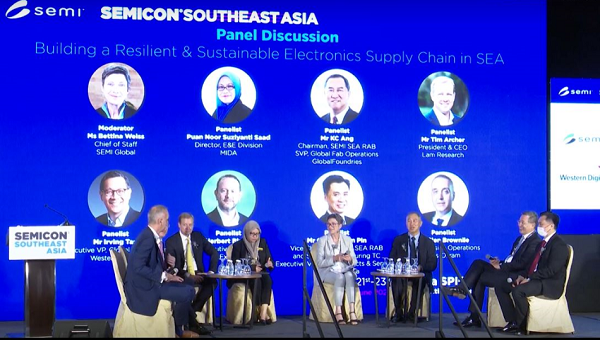
The electronics supply chain recently gathered together at SEMICON Southeast Asia, a premier event that promotes growth of the semiconductor and microelectronics ecosystem in the region. Held June 21-23 in Penang, Malaysia, the theme of this year’s show was “Building a resilient and sustainable electronics supply chain in Southeast Asia.”
Lam was pleased to be a diamond sponsor, and also had a popular booth in the expo hall. Lam President and CEO Tim Archer gave a talk and was a panelist at the CxO summit. Lam technologists and other representatives also participated in the show. Below are some of the highlights of what they shared.
1. At the CxO Summit, Tim shared that wafer throughput generally increases by using more energy in wafer fabrication equipment. Today, as sustainability becomes an increasingly important design factor, the industry will need to develop creative solutions that allow for energy conservation in its products and processes.
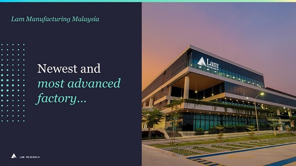
2. Our newest and most advanced factory, located in Penang, Malaysia, isn’t just advanced from a technology perspective, but from a sustainability perspective as well. It is operating on 100% renewable energy today, said Tim during his talk.
3. Another highlight that Tim noted was that Lam Manufacturing Malaysia’s leadership team is taking a leading role toward inclusion and diversity with 50% of its team comprising female employees.
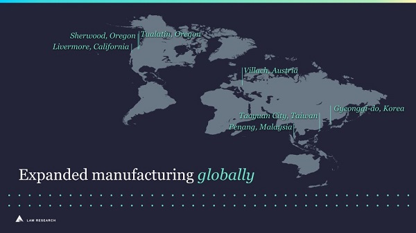
4. To meet the explosive demand for semiconductors, in just two years, Lam will have increased our manufacturing footprint by 50%, expanding every single one of our manufacturing facilities around the globe.
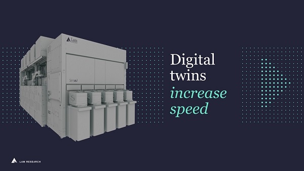
5. For the industry to continue solving society’s challenges, greater collaboration is needed. Digital twins (virtual representations) of Lam’s products and virtual process development are two of the tools to that can help increase speed to solution.
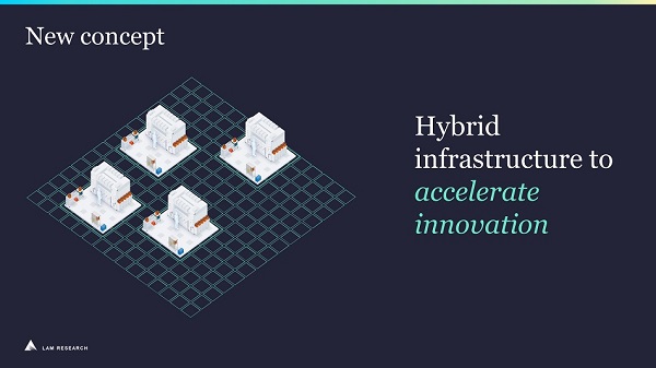
6. The industry is already innovating at breakneck speed – but we want to go even faster. Tim described how we are reimagining how we work so that we can deliver disruptive technologies faster and more often.
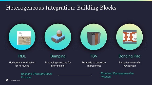
7. One of the leading techniques actively pursued in advanced packaging today is chiplets heterogenous integration (HI). CheePing Lee, advanced packaging technical director, explained that HI, which brings multiple chips (or chiplets) together into a single package, can leverage advanced wafer manufacturing technologies.
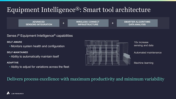
8. An intelligent semiconductor manufacturing tool is one that is self-aware, self-maintained, and adaptive, shared Jason Shields, VP of Equipment Intelligence®. By using big data and associated artificial intelligence technologies, such tools can improve manufacturing productivity and yield.
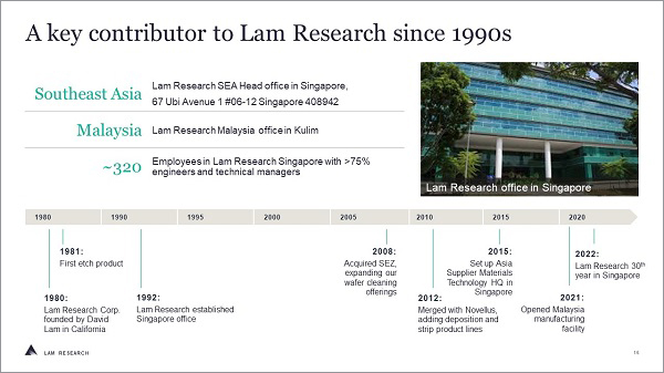
9. Lam has been in the region since 1992, when the Singapore office opened, observed Jonathan Heng, strategic marketing program manager of advanced packaging.
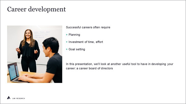
10. Speaking at the Workforce and Development Pavilion, Zaiem Meah, Human Resources director, introduced the concept of a career board of directors as a way to support professional growth.