This month, copper interconnects turned 20. That’s probably something like 200 in “technology years” considering the pace of innovation today. Yet even after 20 years of advances in chipmaking technology, the copper revolution is still considered one of the most significant inflections the industry has ever seen. Thanks to the integration of copper, electronic products have been getting faster, more capable, and more affordable ever since. In recognition of this important milestone, we look back at what was going on in the industry at the time and what it took to successfully integrate copper.
Aluminum Scaling Stalls
Integrated circuits (ICs) initially used aluminum as a conductor and silicon dioxide as an insulator (dielectric) to create the interconnect layers that electrically connect or wire individual devices together. Aluminum was deposited across the wafer surface, then selectively etched to form the wiring pattern. The oxide insulator was next deposited, and chemical mechanical planarization (CMP) flattened the rough surface to complete a set of interconnect steps.

As device features continued to shrink in the late 1980s, ever thinner aluminum lines could no longer deliver the speed and electrical integrity performance required. A better-performing conducting material was needed to continue shrinking device dimensions, as well maintain the cost benefits that chipmakers expected. For years, the industry had been roughly following the Moore’s Law pace of doubling transistor density every 18 months, and now aluminum’s electrical limitations were driving that scaling to a halt. This led the industry to begin investigating alternatives.
Copper Presents Challenges
Copper was soon being considered as it offered lower resistivity, enabling faster device speed. It also provides better reliability since it is not as vulnerable as aluminum to electromigration. In this phenomenon, the electric current pushes metal atoms in the wiring, which can lead to increased resistance and eventual circuit failure. However, efforts to etch copper using a plasma (charged gas) process led to a dead end. Copper does not readily form volatile compounds, so it can’t be removed easily from the wafer surface by converting it to a gaseous state. Thus, either a suitable new conductor, a radically different patterning process, or both were needed to continue scaling.
Copper’s electrical characteristics made it such a superior choice relative to other conductor candidates, that the industry continued working on it. Engineers began considering a damascene process – borrowed from the jewelry industry, where in the city of Damascus, precious metals were inlaid into patterns etched into a base metal. Instead of etching copper, the idea was to first deposit and etch the dielectric material, forming a pattern of trenches and via holes (i.e., a mold for the inlaid metal). Then, rather than depositing a film of metal across the entire wafer surface, only the pattern would be filled with metal.

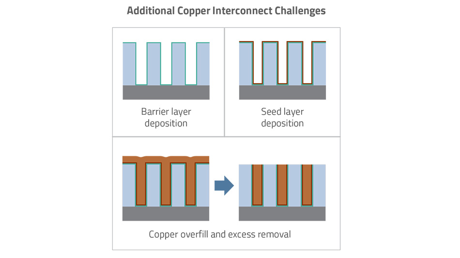
In addition to the obvious need to re-engineer chip designs, many challenges had to be addressed to integrate such a radically different process. Initially, many types of physical vapor deposition (PVD) and chemical vapor deposition (CVD) processes were tested for the copper fill step, but all failed. Likewise, a special metal plating process had to be developed for the high aspect ratio or tall, narrow pattern features involved in the damascene technique. Since copper atoms could diffuse into the dielectric and degrade the desired insulating property, any copper interconnect solution would require a barrier layer to protect the dielectric. This barrier would need a thin electrically conducting seed layer on top of the barrier to get the plating process to start. Finally, metal CMP had to be developed to remove the excess copper deposited during the fill process. Oh, and the pressure was on for all these changes to be integrated quickly, of course, to stay on the Moore’s Law trajectory.

Collaboration Speeds Solution
Fast-forward to around 1995. At this point, IBM and Novellus Systems (now part of Lam) were collaborating on an electrochemical deposition (ECD) or metal plating process for copper. IBM contributed the electroplating solution that enabled copper to be plated from the bottom up without voids in the high aspect ratio features. The process (later known as Novellus’ Electrofill™) was used on what would become the SABRE® family of metal plating tools. Novellus led a “Damascus Alliance” to address key integration issues and speed process adoption. This alliance included Lam, whose dielectric etch equipment created the pattern later filled by copper, two CMP suppliers, and a post-CMP wafer clean supplier.
Then, on June 2, 1998, the “Damascus” production-ready damascene process was announced. Of note, the solution involved eight tools, eight critical steps, and four suppliers all working together to support chipmakers’ transition to copper – collaboration on a scale rarely seen. Shortly thereafter, chipmakers began replacing aluminum with copper for the interconnect layers as the “Age of Damascene” began.
Since then, copper has been the interconnect material of choice. Laid end-to-end, there can be ~30 miles of interconnect in advanced chips. To address performance and reliability requirements in the most advanced semiconductor devices, some of the narrowest (densest) interconnect layers have switched from copper to cobalt – a transition enabled by SABRE. New technologies and new collaborations are also being pursued to enable copper extendibility to the 5 nm node and even beyond. Copper will almost certainly be used in the upper interconnect layers for another 20 years, due to its high electrical conductivity, and we look forward to celebrating another copper milestone anniversary.