Addressing critical needs for next-generation 3D NAND and DRAM devices, Lam has developed the industry’s first all-atomic layer deposition (ALD) low-fluorine tungsten (LFW) fill process with its new ALTUS® Max E Series system. As memory chipmakers move to smaller technology nodes, they are facing additional scaling and integration challenges. For tungsten deposition, device structures have higher aspect ratios and are increasing narrow, making it more difficult to completely fill these features and minimize resistance.
Historically, one approach used to lower resistance has been to make the underlying TiN (titanium nitride) barrier film thinner. For next-generation memory designs, however, these barriers are becoming too thin to protect the neighboring insulating layers from attack by fluorine that migrates from the tungsten films. In addition, as 3D NAND manufacturers add more memory cell layers to increase storage capacity, the stress due to the taller film stack can cause excessive wafer bowing. These unwanted defects and stress can ultimately impact yield and device performance.
As described in the recent announcement below Lam’s new LFW ALD process resolves these issues by lowering fluorine content, stress, and resistivity while delivering the required fill performance and productivity. ALTUS Max E Series is the latest addition to Lam’s market-leading deposition and etch solutions for 3D NAND and DRAM manufacturing.
Lam Research Enables Next-Generation Memory with Industry’s First ALD Process for Low-Fluorine Tungsten Fill
New ALTUS® Max E Series delivers low-fluorine, low-stress, and low-resistivity 3D NAND and DRAM solution with high productivity
FREMONT, CA — (Marketwired) – 8/9/16 – Lam Research Corp. (NASDAQ: LRCX), an advanced manufacturer of semiconductor equipment, today introduced an atomic layer deposition (ALD) process for depositing low-fluorine-content tungsten films, the latest addition to its industry-leading ALTUS® family of products. With the industry’s first low-fluorine tungsten (LFW) ALD process, the ALTUS Max E Series addresses memory chipmakers’ key challenges and enables the continued scaling of 3D NAND and DRAM devices. Building on Lam’s market-leading product portfolio for memory applications, the new system is gaining market traction worldwide, winning production positions at leading 3D NAND and DRAM manufacturers and placement at multiple R&D sites.
“Consumer demand for ever more powerful devices is driving the need for high-capacity, high-performance storage, and deposition and etch are key process technology enablers of advanced memory chips,” said Tim Archer, Lam’s chief operating officer. “With the addition of the ALTUS Max E Series, we are expanding our memory portfolio and enabling our customers to capitalize on this next wave of industry drivers. Over the past twelve months, as the 3D NAND inflection has accelerated, we have doubled our shipments for these applications, leading to the largest deposition and etch installed base in our 3D NAND served markets.”
As manufacturers increase the number of memory cell layers for 3D NAND, two issues have become apparent for tungsten deposition in the word line fill application. First, fluorine diffusion from the tungsten film into the dielectrics can cause physical defects. Second, higher cumulative stress in devices with more than 48 pairs has resulted in excessive bowing. The resulting defects and stress can cause yield loss, as well as degraded electrical performance and device reliability. Because of these issues, tungsten films for advanced 3D NAND devices must have significantly reduced fluorine and intrinsic stress. Further, as critical dimensions shrink, resistance scaling becomes more challenging for the DRAM buried word line, as well as for metal gate/metal contact applications in logic devices.
“As memory chip manufacturers move to smaller nodes, the features that need to be filled are increasingly narrow and have higher aspect ratios,” said Sesha Varadarajan, group vice president, Deposition Product Group. “Lam’s new LFW ALD solution uses a controlled surface reaction to tune stress and fluorine levels and to lower resistance, all while delivering the required tungsten fill performance and productivity. When compared to chemical vapor deposition tungsten, the ALTUS Max E Series lowers fluorine content by up to 100x, lowers stress by up to 10x, and reduces resistivity by over 30%, solving some of our customers’ most critical scaling and integration challenges.”
The ALTUS Max E Series with LFW ALD technology offers a unique all-ALD deposition process that leverages Lam’s PNL® (Pulsed Nucleation Layer) technology, which is the industry benchmark for tungsten ALD with 15 years of market leadership and more than 1,000 modules in production. Lam led the transition of chemical vapor deposition (CVD) tungsten nucleation to ALD tungsten nucleation with its PNL technology. The company continued that leadership by advancing low-resistivity tungsten solutions with its products ALTUS® Max with PNLxT™, ALTUS® Max with LRWxT™, and ALTUS® Max ExtremeFill™ for enhanced fill performance.
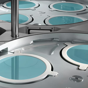
The ALTUS products use Lam’s quad-station module (QSM) architecture to allow per-station optimization of tungsten nucleation and fill for fluorine, stress, and resistance without compromising fill performance since station temperature can be set independently. The QSM configuration also maximizes productivity of the all-ALD process by providing up to 12 pedestals per system, enabling the highest footprint productivity in the industry.
For more announcements from Lam, please visit our Newsroom Home or Press Releases web pages.