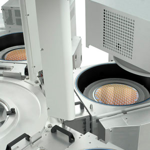
With the introduction of Lam’s latest Flex™ dielectric etch system, we have expanded our atomic layer etching (ALE) portfolio to include both conductor and dielectric etch. At the 10 nm technology node and beyond, conventional technologies do not provide sufficient control for the stringent specifications demanded. As described in our recent announcement , this newest Flex product delivers the atomic-level control needed for manufacturing advanced logic devices and is first in the industry to use dielectric ALE in high-volume production.
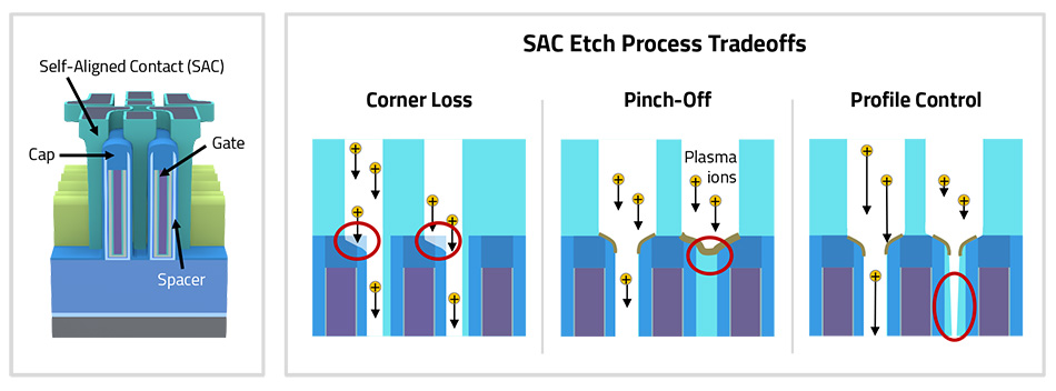
As logic devices continue to scale, precise and repeatable etching is needed to achieve the required feature characteristics. For example, as transistors get smaller and are packed more closely together, there is less room available for forming and electrically isolating the contact, leading to the adoption of self-aligned contacts (SACs). As a result, contact etch has become one of the most critical processes, directly impacting both wafer yield and transistor performance.
SAC Etch Challenges
Given the complex and tight geometries involved, the SAC etch process is particularly challenging. Achieving the overall desired results involves optimizing three key tradeoffs. First is corner loss: poor etch selectivity (the rate of removing one material versus another) can lead to unwanted erosion of the spacer film’s corners. Second is pinch-off: polymer chemistries may be used to protect the spacer, but too much polymer can completely pinch off, or block, the contact opening. Third is profile control: polymer buildup at the top of the contact can prevent plasma ions from reaching the bottom, resulting in an undesirable tapered profile (wider at the top than at the bottom).

ALE Solution
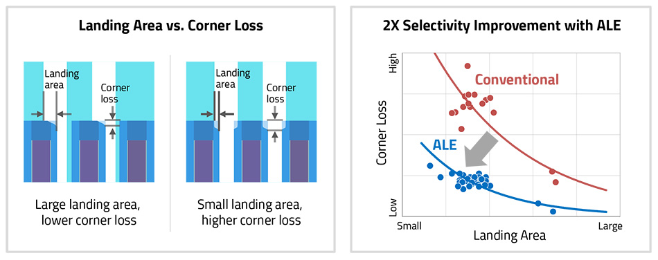
Lam’s latest ALE process for dielectric films like silicon dioxide (SiO2) delivers the control needed to manage these tradeoffs. Directional (anisotropic) etch and high selectivity enable the contact profile to be shaped accurately without damaging the adjacent spacer. Lam’s ALE process has demonstrated 2x better selectivity versus conventional techniques, providing with lower spacer corner loss regardless of landing area variation.

With ALE, literally a few layers of atoms are removed at a time by using cyclical deposition and removal steps. As a result, ALE provides a level of control that breaks the process tradeoff challenge for SAC and provides enabling capability for other critical dielectric etch applications.
To see how atomic-layer processing works, watch our video, “Building Chips a Few Atoms at a Time.” To learn more about ALE, read our article, “Moving atomic layer etch from lab to fab,” in Solid State Technology.