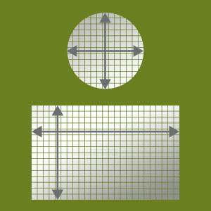
Panel-level fan-out chip manufacturing – using large square or rectangular substrates instead of wafers – is being developed as a means to lower the cost of back-end processes for some packaging applications. Lam authors Choon Lee, Tom Bondur, and Manish Ranjan share their thoughts on this innovative approach in Chip Scale Review.
The era of “More than Moore” has extended to the packaging world. Packaging plays a critical role in improving electrical and thermal performance and power consumption. Recently developed packaging technologies such as high-density wafer-level fan-out (WLFO) packaging have gained increased attention as a way to meet performance and form factor requirements in the semiconductor market. To ensure broad adoption for this packaging technology, several foundry and outsourced semiconductor assembly and test (OSAT) companies are considering the use of larger panel size substrates. This article will discuss some of the cost motivation and performance challenges associated with the use of panel substrates for fan-out wafer-level packaging.
Today, packaging is enabling advances in consumer electronics such as smartphones by enabling more transistors on a smaller area. For example, in the iPhone 7, the Apple applications processor has around 150% more transistors even though the chip has increased by only 20%. For reference, the chip has approximately 3.3 billion transistors in a chip with an area of 125 mm2.
This latest generation of applications processors is manufactured using a technology called “integrated fan-out,” which is based on high-density WLFO. Several key building blocks for this packaging technology include multiple redistribution layers and mega pillars to support the package-on-package (PoP) structure. Packaging innovations include the use of mega pillars with 200 um diameter and 200 um height instead of a through-mold via (TMV) for a typical PoP structure. Furthermore, the top-level memory package height was reduced using a side-by-side arrangement of LPDDR4 memories (instead of conventional memory die stacking), and the impressive introduction of 0.3 mm ball pitch for the first time in memory history. Lastly, this technology introduction eliminated the use of flip-chip substrates, thereby enabling a reduction in overall package height. At the 2016 ICEP conference in Sapporo, Japan, Google demonstrated the advantages associated with the combination of application processor and memory in a planar layout to boost memory performance and reduce power usage. It is evident that the use of packaging technology for enabling next-generation system-level performance is gaining increased focus from several top-tier semiconductor device and fabless suppliers.
Continue reading the article on the Chip Scale Review website.