| Su | Mo | Tu | We | Th | Fr | Sa |
|---|---|---|---|---|---|---|
| Su | Mo | Tu | We | Th | Fr | Sa |
|---|---|---|---|---|---|---|


 |Nov 30, 2020|
Filling complex, high aspect ratio structures is a challenge for 3D NAND, DRAM, and logic chipmakers. Lam’s Aaron Fellis, vice president and general manager of dielectric atomic layer deposition...

 |Oct 26, 2020|
When they were first commercialized at the 22 nm node, finFETs represented a revolutionary change to the way we build transistors, the tiny switches in the “brains” of a chip. As compared to...

 |Oct 19, 2020|
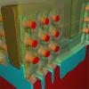
Semiconductor process development is no easy task, with each generation of devices more difficult and expensive to create. Traditional cycles of build-and-test development are becoming obsolete,...

 |Oct 12, 2020|
Lam’s newest product in its line of GAMMA® dry photoresist strip systems, brings the performance of the GAMMA® GxT® 300 mm to 200 mm wafer processing. The GAMMA GxT has been specifically...

 |Sep 21, 2020|
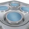
In today’s press release below, Lam announced the new Striker® FE platform featuring its patented ICEFill™ technology, which provides bottom-up filling in complex high aspect ratio (HAR)...