| Su | Mo | Tu | We | Th | Fr | Sa |
|---|---|---|---|---|---|---|
| Su | Mo | Tu | We | Th | Fr | Sa |
|---|---|---|---|---|---|---|


 |Apr 12, 2023|
The journal Nature publishes Lam’s groundbreaking study. Rick Gottscho and Keren Kanarik share what it means for Lam and the semiconductor industry.

 |Mar 22, 2023|
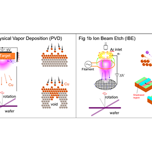
Introduction Cu’s resistivity depends on its crystal structure, void volume, grain boundaries and material interface mismatch, which becomes more significant at smaller scales. The formation of...
-
 |Mar 17, 2023|
System in Package (SiP) requirements push substrate designs to smaller features (similar to FO-PLP). Convergence in requirements allows shared R&D costs for panel level processing systems.

 |Mar 3, 2023|
Soumya has automated Lam’s product software testing and processes for 19 years. The software she works on allows us to validate the behavior of our tool's software at any fab remotely. Soumya...

 |Feb 28, 2023|
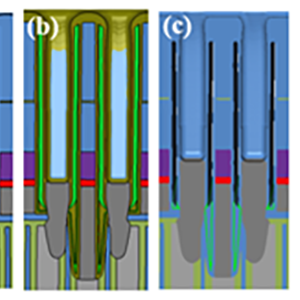
With decreasing dynamic random-access memory (DRAM) cell sizes, DRAM process development has become increasingly difficult. Bit-line (BL) sensing margins and refresh times have become problematic...