| Su | Mo | Tu | We | Th | Fr | Sa |
|---|---|---|---|---|---|---|
| Su | Mo | Tu | We | Th | Fr | Sa |
|---|---|---|---|---|---|---|


 |Jan 13, 2023|
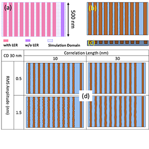
Line edge roughness (LER) can occur during the exposure step in lithography [1-2]. Similarly, etch and deposition process steps can leave a roughness on semiconductor surfaces. LER is a stochastic...

 |Nov 8, 2022|
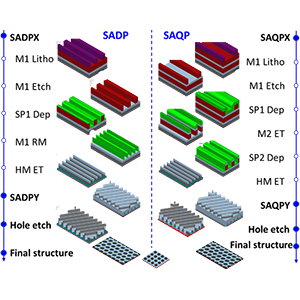
Introduction The semiconductor industry has been focused on scaling and developing advanced technologies using advanced etch tools and techniques. With decreasing semiconductor device dimensions...
 |Oct 27, 2022|
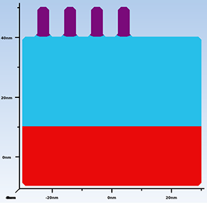
Reducing the parasitic capacitance between the gate metal and the source/drain contact of a transistor can decrease device switching delays. One way to reduce parasitic capacitance is to reduce...

 |Sep 22, 2022|
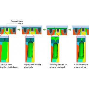
With continuous device scaling, process windows have become narrower and narrower due to smaller feature sizes and greater process step variability [1]. A key task during the R&D stage of...

 |Aug 18, 2022|
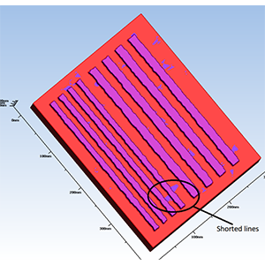
Introduction BEOL metal line RC delay has become a dominant factor that limits chip performance at advanced nodes [1]. Smaller metal line pitches require a narrower line CD and line-to-line...