| Su | Mo | Tu | We | Th | Fr | Sa |
|---|---|---|---|---|---|---|
| Su | Mo | Tu | We | Th | Fr | Sa |
|---|---|---|---|---|---|---|


 |Jul 10, 2017|
The demands of our modern world for more connectivity, functionality, and capacity from our electronic devices – alongside the seemingly endless imagination for new applications – are pushing...
 |Jul 3, 2017|
If you’re part of the semiconductor industry, you know there are few better networking and technical sharing venues than the SEMICON tradeshows, and SEMICON West is no exception. Being held in...

 |Jun 12, 2017|
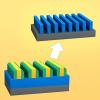
Used to extend the capabilities of conventional lithography, multiple patterning is a process of overlaying patterns of larger dimensions to achieve smaller and/or more tightly packed features. In...

 |May 15, 2017|
Imagine being able to deposit a film of material just a few atomic layers at a time. As impossible as that sounds, atomic layer deposition (ALD) is a reality. In fact, it’s being used in an...

 |Apr 10, 2017|
Southeast Asia is a major hub for the chip industry’s assembly, packaging, and test services – back-end manufacturing processes that are becoming an increasingly important topic of discussion....