| Su | Mo | Tu | We | Th | Fr | Sa |
|---|---|---|---|---|---|---|
| Su | Mo | Tu | We | Th | Fr | Sa |
|---|---|---|---|---|---|---|


 |Aug 24, 2021|
We play a critical role in driving semiconductor breakthroughs for the next generation. Since 2015, Unlock Ideas has been an integral program to unleash the power of innovation by providing gifts...

 |Aug 16, 2021|
From August 23-27, our experts will join industry leaders at SEMICON Southeast Asia, to discuss semiconductor advancements in an era of 5G and next-generation technologies. Themed “Powering...

 |Aug 9, 2021|
As a materials engineer, I am very proud of the fact that key advances in human civilization have been driven by materials innovation. The stone age, bronze age and iron age were all essential...

 |Jul 26, 2021|
There’s a lot of talk about the Internet of Things (IoT) and its impact on our day-to-day lives. From home security systems to smart watches, IoT is upgrading the technologies we rely on every...

 |Jul 19, 2021|
Helium gas is increasingly in short supply. While consumers may be most familiar with it for use in filling balloons, it is used much more heavily in a variety of industrial processes –...

 |Jul 12, 2021|
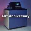
Back in 1981, Lam pioneered single-wafer plasma etch tools with its first product, the Lam AutoEtch 480 plasma etcher. Introduced as “a streamlined plasma etching system designed specifically...
 |Jul 6, 2021|
The IEEE International Interconnect Technology Conference (IITC) will be held July 6-9, 2021, as a hybrid event – virtual and in-person (Kyoto Research Park, Kyoto, Japan), with on-demand...

 |Jun 21, 2021|
Preventative Maintenance “What is wet, but dry?” might sound like a riddle, and the answer for plasma process tools are “wet cleans,” an important type of preventative maintenance. The...
 |Jun 14, 2021|
Chip features continue to shrink to incredibly small dimensions and different device architectures are being devised to supply consumers with more powerful electronics. Atomic layer deposition...

 |Jun 7, 2021|
The pervasive use of technology has brought about a tremendous growth in data as well as an explosion in scaling and complexity of integrated circuits. That trend continues as the focus on...