| Su | Mo | Tu | We | Th | Fr | Sa |
|---|---|---|---|---|---|---|
| Su | Mo | Tu | We | Th | Fr | Sa |
|---|---|---|---|---|---|---|


 |Feb 27, 2025|
DWMG structures can help improve DRAM by reducing energy waste. These structures fix a known flaw called “gate-induced drain leakage” (GIDL).
-
 |Feb 19, 2025|
Lam’s latest etch tool, called Akara®, is a significant achievement that helps enable the future of semiconductors requiring small, complex structures. Akara uses proprietary plasma processing technologies to deliver a high degree of etch process control and responsiveness that goes beyond the capabilities of mainstream plasma etch technologies.
-
 |Feb 13, 2025|
Lam has developed the world's only EUV dry resist deposition and dry development technologies with capabilities that support leading-edge pattern fidelity, defectivity, material usage, and overall cost of ownership.
-
 |Jan 31, 2025|
To evaluate stress and mitigate its effects, predictive 3D process models can be used to predict the impact of mechanical stress on yield and performance.
-
 |Dec 12, 2024|
Virtual twin technologies can reduce the carbon footprint of the tool R&D process.

 |Dec 11, 2024|
Lam’s university collaborations supports Lam’s technology pipeline and talent pipeline with creative approaches to industry challenges.

 |Oct 22, 2024|
AR and VR are helping the company shift left and ramp for the $1 trillion industry Lam’s adoption of immersive technologies is expected to beat today’s KPIs by 20% Driving the news: With the...
 |Aug 15, 2024|
Learn about three key semiconductor markets and Lam’s role in supporting our customers Find out what innovative technology is driving each market and Lam’s tools that help enable it Lam...
 |Nov 16, 2023|
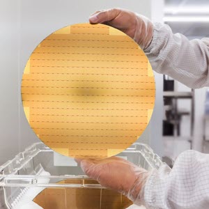
Nearly all microchips begin as slices of highly purified silicon.
 |Aug 7, 2023|
The terms “fab” and “foundry” are often used interchangeably, but that’s technically incorrect. Knowing the difference is important so you can better understand the semiconductor ecosystem.