Month Year
| Su | Mo | Tu | We | Th | Fr | Sa |
|---|---|---|---|---|---|---|
Month Year
| Su | Mo | Tu | We | Th | Fr | Sa |
|---|---|---|---|---|---|---|


 |Aug 9, 2023|
Lam Research and the Centre for Nano Science and Engineering (CeNSE) at the Indian Institute of Science (IISc) partner to train up to 60,000 semiconductor engineers.

 |Jul 14, 2023|
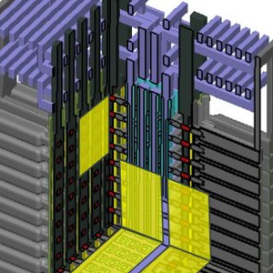
DRAM is following NAND in going 3D, but architecture needs are unique and challenging. 3D DRAM is needed to keep up with the demands of graphics cards, portable devices, and more. Here's an idea of how to architect it.

 |Jun 22, 2023|
Up to 60,000 engineers in India to be trained on Lam’s unique virtual fabrication platform
 |Jun 22, 2023|
New portfolio joins physical and virtual semiconductor worlds into a single ecosystem
-
 |Jun 20, 2023|
Addresses key manufacturing challenges and significantly improves wafer yield Builds on Lam's 15-year heritage of innovation in bevel solutions