| Su | Mo | Tu | We | Th | Fr | Sa |
|---|---|---|---|---|---|---|
| Su | Mo | Tu | We | Th | Fr | Sa |
|---|---|---|---|---|---|---|


 |Feb 16, 2023|
SEMICON Korea 2023 kicked off with a keynote speech, “Accelerating Innovation – From Lab to Fab,” delivered by Pat Lord, EVP of the Customer Support Business Group and Global Operations. Pat...

 |Feb 2, 2023|
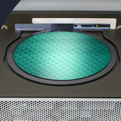
Metryx marked 200th tool shipment by donating science equipment to a local high school

 |Jan 13, 2023|
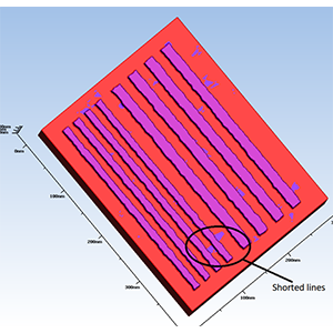
Line edge roughness (LER) can occur during the exposure step in lithography [1-2]. Similarly, etch and deposition process steps can leave a roughness on semiconductor surfaces. LER is a stochastic...

 |Dec 19, 2022|
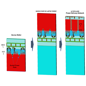
At the beginning of my career in semiconductor equipment, the backside of the wafer was a source of anxiety. In one memorable instance in my early career, several wafers flew off a robot blade...
- |Nov 21, 2022|
“Engineering a Greener Fab” was the theme of the Lam Research Technical Symposium, Lam’s premiere forum for intellectual and scientific sharing.